Clear Sky Science · en
Electrical control of the metal-insulator transition in a one dimensional device
Turning Electricity into a Nano-Scale On/Off Switch
Modern electronics already shrink transistors to astonishingly small sizes, but quantum technologies demand even finer control: not just turning current on and off, but sculpting the very energy landscape that electrons feel. This paper shows that engineers can now use tiny electrical knobs to drive a single carbon nanotube—a cylinder of carbon atoms only a few nanometers wide—from a metal-like conductor into an insulator and back again, all by design. That kind of switchable behavior, achieved in a clean and predictable way, is a key ingredient for building future quantum devices that are both powerful and robust.
A One-Dimensional Wire with Many Tiny Knobs
At the heart of the experiment is a suspended carbon nanotube that acts as an ultra-thin, nearly one-dimensional wire. Instead of resting directly on a surface, the nanotube is stretched between two metallic contacts, like a tightrope. Beneath it lies a row of 15 narrow electrodes, arranged like the keys of a piano. Each of these “keys” can be set to its own voltage, allowing the researchers to shape the electrical potential along the nanotube with great precision. By applying alternating voltages to neighboring gates, they impose a repeated pattern—high, low, high, low—that mimics how atoms in a crystal create a periodic landscape for electrons. 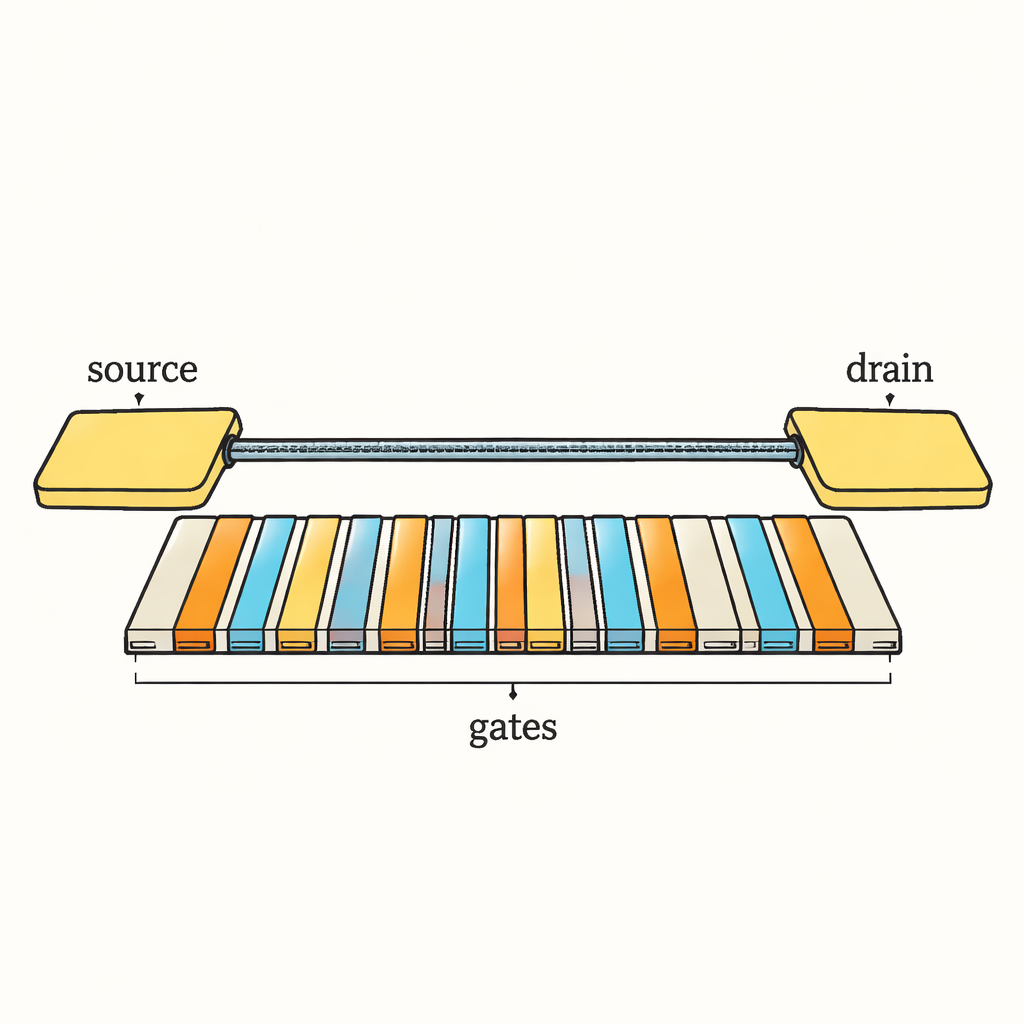
From Free-Flowing Current to a Quiet, Gapped State
To see how the nanotube responds, the team measures how easily current flows through it at very low temperatures, just a few hundredths of a degree above absolute zero. With only a weak modulation of the gate voltages, the device behaves much like a familiar single-electron transistor: current is blocked only in small ranges of voltage due to charging effects, but otherwise electrons can pass through. When the researchers increase the amplitude of the alternating gate pattern, the picture changes dramatically. A wide region of almost zero conductance appears around zero bias, signaling that electrons now face a genuine energy gap rather than just isolated charging barriers. By analyzing these measurements with a standard transport model, they show that this gap acts as a single-particle property of the nanotube’s spectrum, not a side effect of strong electron–electron repulsion.
Designing a Synthetic Crystal and Its Energy Bands
The experiment is guided by classic theory dating back to the early 1950s, which describes electrons moving in a smoothly wavy, cosine-shaped potential. In such a landscape, electrons form energy bands separated by gaps whose sizes depend on how strong the modulation is. Using realistic parameters for their device, the authors calculate how the first few gaps should grow as the alternating gate voltage increases. For small modulations, the gap should scale roughly in proportion to the voltage; for larger ones, it grows more like the square root of that voltage, reflecting how electrons become confined in deep wells similar to harmonic oscillators. 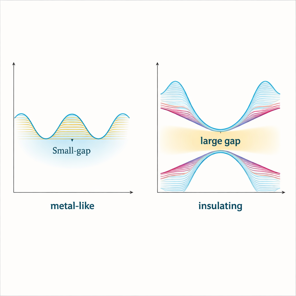
How Many Gates Make a True Insulator?
One practical question is how long such a patterned region must be before a robust insulating gap appears. The team answers this by turning on the alternating voltages gate by gate, effectively building the synthetic crystal site by site. With only a few active gates, the conductance shows local irregularities but no clear, tunable gap. Once seven or more gates participate, a well-defined gap emerges and then remains essentially stable as more gates are added. This demonstrates that the insulating state is a collective property of a sufficiently long chain, not just the result of a single deep trap or hidden defect, and that the engineered potential is remarkably uniform along the nanotube (variations in the gap are only on the order of 15 percent).
Why This Matters for Future Quantum Technologies
In everyday terms, the researchers have built an electrically programmable barrier in a one-dimensional quantum wire—a barrier whose height and width can be dialed in at will. Such controllable energy gaps are a vital building block for exotic quantum states that live at the ends of one-dimensional systems and are thought to be useful for fault-tolerant quantum computing. Because this carbon nanotube device is already integrated in a microwave cavity, it also opens doors to using light to probe and manipulate these states. More broadly, the same strategy could be applied to other low-dimensional materials, providing a flexible platform for simulating complex condensed-matter phenomena, from charge density waves to the elusive “Peierls instability,” all on a chip.
Citation: Craquelin, J., Jarjat, L., Hue, B. et al. Electrical control of the metal-insulator transition in a one dimensional device. Nat Commun 17, 1629 (2026). https://doi.org/10.1038/s41467-026-68344-0
Keywords: carbon nanotube, metal-insulator transition, energy gap, quantum devices, topological chains