Clear Sky Science · en
Measuring the molecular origins of stiffness in organic semiconductors
Why the stiffness of soft electronics matters
Flexible electronics—such as bendable displays, wearable health sensors, and soft solar cells—rely on organic semiconductors that behave a bit like plastic and a bit like metal. We already know a lot about how well these materials conduct electricity, but far less about how stiff or soft they are at the scale of individual molecules. This article explores how tiny changes in molecular design can subtly tune stiffness, and how those changes might ultimately affect the performance and reliability of future flexible devices.
From bendable films to molecular-scale feel
At the scale of a phone screen, organic semiconductors are famously flexible, but this study asks a deeper question: how stiff are they on the nanometre scale, where individual molecules pack together? To probe this, the researchers focus on a widely studied semiconductor called DNTT and several close chemical cousins with added “side chains”—extra molecular tails that are expected to soften the material. Measuring such delicate effects is difficult, because the very act of pressing on a soft surface with an atomic force microscope (AFM) can disturb it. The team set out to design measurements precise enough to reveal real molecular trends rather than artefacts of the probing tool itself.
Using a nanoscale finger to feel stiffness
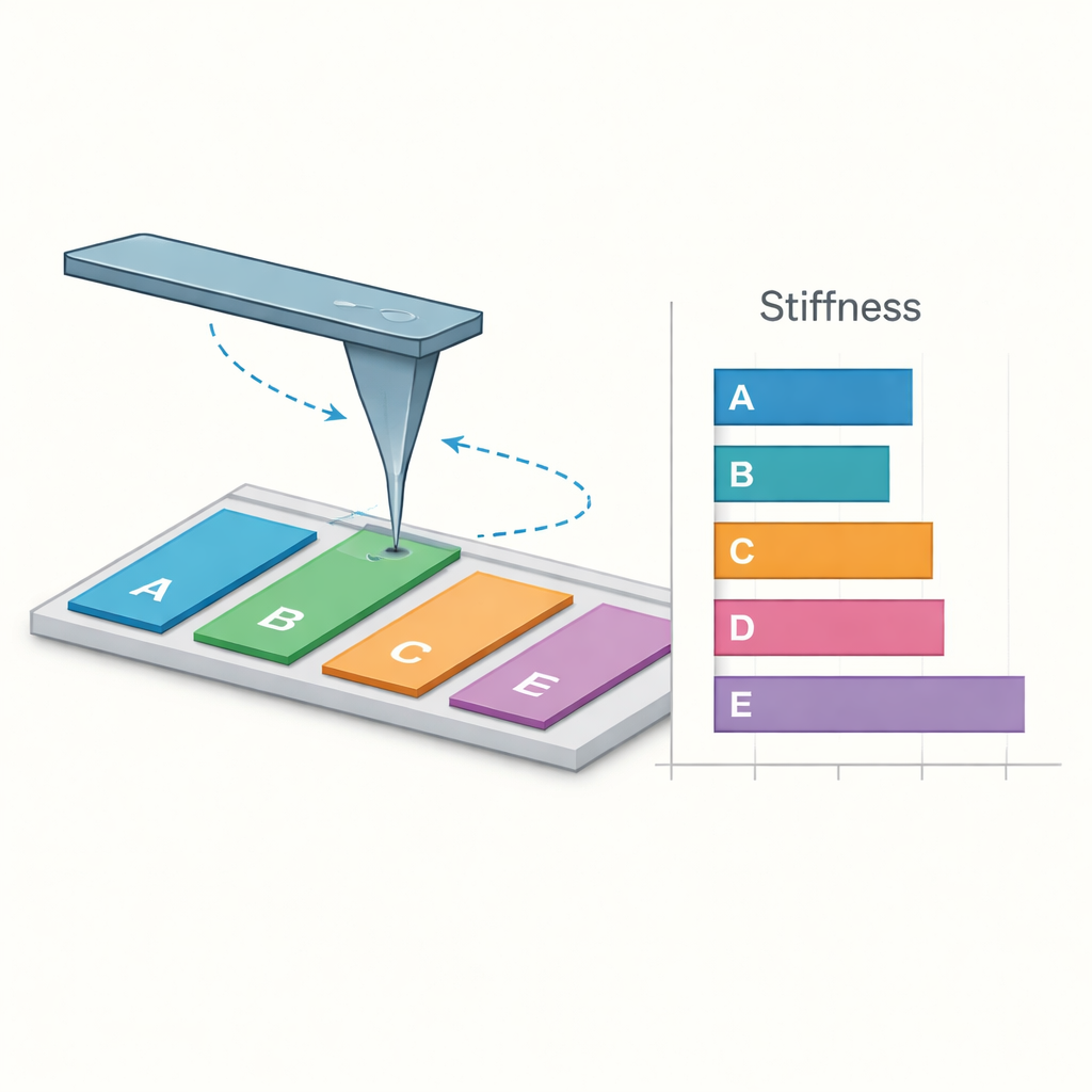
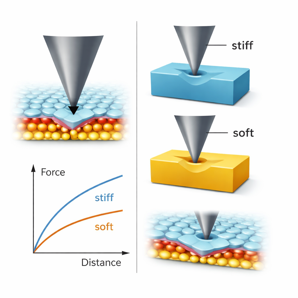
An AFM can be thought of as a nanoscale record-player needle that moves across a surface. Here, the tip is repeatedly pushed down and pulled back at thousands of points across thin films of DNTT and its derivatives. By tracking the full force–distance curve as the tip approaches, indents, and retracts, the scientists extract how much the surface resists indentation, a direct measure of local stiffness. They map these values over areas ranging from several micrometres down to a few hundred nanometres, achieving a spatial resolution of roughly ten nanometres—small enough to sense differences between crystalline domains and their boundaries without averaging everything together.
Cleaning up hidden measurement traps
Because the films are made of small organic molecules, the AFM tip can easily pick up loose material, changing shape mid-experiment. The authors show that contaminated tips give misleading signals: they can double the apparent stiffness, increase adhesion, and even produce force curves that mimic “negative stiffness.” Using simulations and simple geometric models, they demonstrate how tiny sideways slips of the tip—less than a nanometre—can be misread as vertical motion, corrupting the data. By working at moderate forces, monitoring indentation depth and adhesion, and frequently renewing and calibrating tips, they establish a protocol that filters out these spurious effects and isolates the true mechanical response of the molecular lattice.
Tuning softness with molecular tails
Once these pitfalls are controlled, a clear, intuitive pattern emerges. Plain DNTT, which packs tightly with only rigid aromatic cores in the vertical direction, is the stiffest. Adding short phenyl groups makes the crystals slightly less dense and softer along the out-of-plane direction. Adding long, flexible alkyl chains softens them further, and chiral versions with subtly bulkier side chains are softest of all. X-ray measurements confirm that these substitutions expand the crystal lattice, especially along the direction where the AFM presses, reducing how many rigid cores fit into a given volume. Computer simulations using density-functional theory and molecular dynamics reproduce the same trend: the calculated Young’s modulus along the vertical axis is higher for unmodified DNTT and lower for the alkylated variant, while in-plane stiffness can actually increase, aligning with known improvements in charge transport.
How stiffness connects to charge-carrying ability
Electrical measurements on transistor devices made from the same materials reveal that some of the softer, side-chain-modified films actually transport charge better within the plane of the film. Previous theory suggests that, along the direction where charges move, a stiffer lattice can reduce disruptive vibrations and support higher mobility. The new work refines this picture: the same molecular tweaks that soften the material vertically can reorganise and stiffen it sideways, where current flows, while also altering how electronic clouds overlap. The study does not claim stiffness alone determines performance, but it shows that mechanical and electronic properties are tightly intertwined and must be considered together when engineering better organic semiconductors.
What this means for future flexible devices
In practical terms, the authors demonstrate that it is now possible to measure very subtle changes in stiffness directly on molecular semiconductor films, provided that AFM artefacts are rigorously controlled. They show that adding soft side chains to a rigid molecular backbone reliably makes the crystal softer in the pressing direction, and that advanced simulations can predict this behaviour. For non-specialists, the key takeaway is that the “feel” of a molecular solid—how stiff or compliant it is on the nanoscale—is not just a curiosity. It is a tunable property that can be designed through chemistry and may play an important role in making flexible, durable, and efficient organic electronic devices.
Citation: Hwang, KH., Brandt, D., Cristofaro, S. et al. Measuring the molecular origins of stiffness in organic semiconductors. Nat Commun 17, 1621 (2026). https://doi.org/10.1038/s41467-026-68328-0
Keywords: organic semiconductors, nanoscale stiffness, atomic force microscopy, flexible electronics, charge carrier mobility