Clear Sky Science · en
Atomic-scale imaging and charge state manipulation of NV centers by scanning tunneling microscopy
Diamond Defects as Tiny Quantum Tools
Many of tomorrow’s quantum technologies may rely on tiny flaws inside ultra-pure diamonds. These flaws, called nitrogen-vacancy (NV) centers, can act like controllable "spins" that store and process quantum information, sense magnetic fields, and communicate using single particles of light. This article explores a new way to actually see and control individual NV centers at the scale of single atoms—an essential step toward building reliable quantum devices from the bottom up.
Why These Diamond Defects Matter
NV centers form when one carbon atom in the diamond is replaced by a nitrogen atom and a neighboring carbon site is left empty. In the right charge state, called NV− (NV minus), this defect behaves like a highly stable quantum bit that can operate even at room temperature. NV centers are already used in research labs to measure tiny magnetic and electric fields and as building blocks for quantum networks. However, scientists have lacked a clear, atom-by-atom view of how each NV center sits in the surrounding crystal and how its local electrical environment affects its performance. Without this microscopic picture, improving device designs has largely been a matter of trial and error.
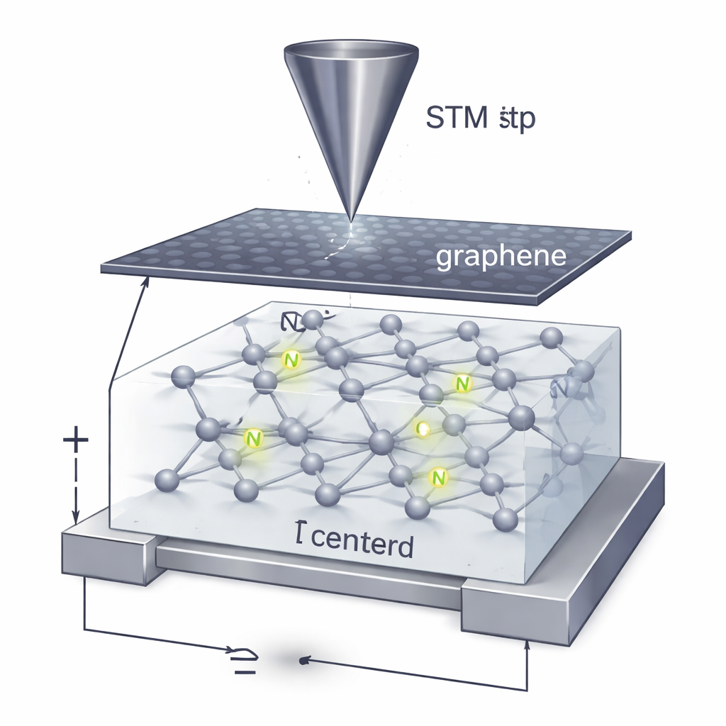
Using a Graphene “Window” to See Inside Diamond
To look directly at individual NV centers, the researchers turned to scanning tunneling microscopy (STM), a technique that can map electronic structure with atomic resolution. STM normally requires an electrically conducting surface, which is a problem for insulating diamond. The team solved this by placing an ultrathin, electrically conductive sheet of carbon—monolayer graphene—on top of the diamond. This graphene layer acts like a transparent window for electrons: it conducts well enough to enable STM measurements, yet is thin and “electronically transparent” enough that the instrument can still sense the buried NV centers underneath.
Fingerprinting Single Defects Atom by Atom
Working at low temperature and under ultra-clean conditions, the authors scanned more than 40 individual defects beneath the graphene-covered diamond surface. By measuring how the electrical conductance changed with applied voltage, they identified a consistent signature for NV− centers: a distinct peak in conductance about 0.3 electronvolts below the Fermi level (the reference energy set by the electrons in the material). Maps of the local electronic density around each defect revealed a two-lobed pattern aligned with the known crystallographic direction of NV centers. This pattern, and the energy position of the peak, allowed the team to distinguish NV− centers from other common defects such as isolated nitrogen atoms (P1 centers), which appeared at very different energies and with different shapes in the STM images.
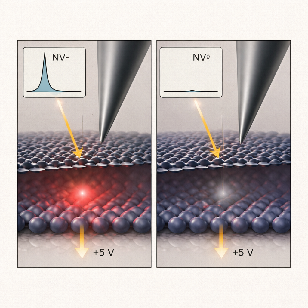
Flipping the Charge of a Single Quantum Defect
Beyond imaging, the most striking advance is the ability to change the charge state of individual NV centers on demand. The researchers parked the STM tip above a chosen NV− center, briefly retracted it, and then applied a strong positive voltage to the diamond. This electric field effectively pulled an electron away from the defect, converting NV− to its neutral form, NV0. After this procedure, the STM images no longer showed the bright defect feature, and the characteristic conductance peak vanished from the spectrum—indicating that the charge state had changed. Importantly, nearby defects just a few tens of nanometers away remained untouched, proving that the manipulation is highly localized. This level of control is about ten times more precise than previous charge-tuning methods in similar systems.
Building Better Quantum Devices from the Bottom Up
In simple terms, this work demonstrates both a microscope and a “tuning knob” for individual quantum defects in diamond. The graphene layer lets STM peer into an insulating crystal to see and characterize single NV centers, while carefully applied voltages allow their charge state to be switched one at a time. These capabilities open a path to designing quantum devices with tailored arrangements of NV centers—densely packed where sensing is needed, and switched off where they would add noise. Future steps may combine this approach with advanced optical techniques, letting scientists correlate atomic-scale images, electrical fingerprints, and light emission from the very same defect. Together, these tools bring us closer to engineering practical solid-state qubits with the precision that modern electronics already enjoys.
Citation: Raghavan, A., Bae, S., Delegan, N. et al. Atomic-scale imaging and charge state manipulation of NV centers by scanning tunneling microscopy. Nat Commun 17, 1617 (2026). https://doi.org/10.1038/s41467-026-68323-5
Keywords: nitrogen-vacancy centers, diamond qubits, scanning tunneling microscopy, graphene interface, quantum sensing