Clear Sky Science · en
Self-aligned and self-limiting van der Waals epitaxy of monolayer MoS2 for scalable 2D electronics
Building Better Electronics with Atom-Thin Materials
Our phones and computers are pushing the limits of what today’s silicon chips can do. To keep shrinking devices while cutting power use, engineers are turning to new, ultra-thin materials only one atom thick. This article shows how researchers have learned to grow large, flawless sheets of one such material—monolayer molybdenum disulfide (MoS₂)—in a way that is compatible with industrial chip factories.
Why Growing a Perfect Atomic Carpet Is So Hard
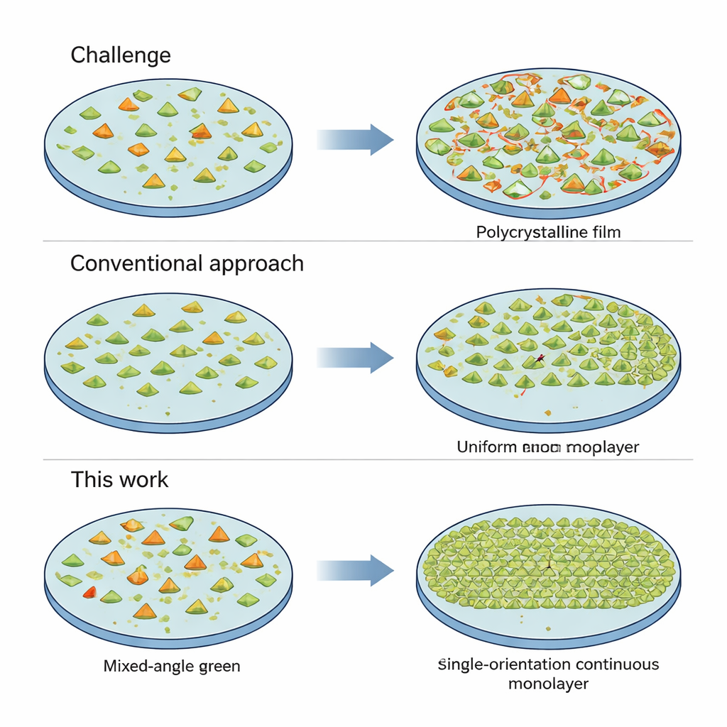
Imagine trying to tile an entire floor with tiny, triangular tiles that must all face the same direction. If some triangles flip or twist a little, the floor ends up full of seams and weak spots. The same problem appears when growing 2D crystals like MoS₂ on sapphire wafers. Earlier methods tried to make every tiny “seed” crystal start in exactly the same direction, then stitch them together. In practice, growth happens under fast, nonequilibrium conditions, and many islands form with opposite or slightly rotated orientations, creating a patchwork of microscopic grains that hurts electronic performance.
A New Self-Aligning Growth Pathway
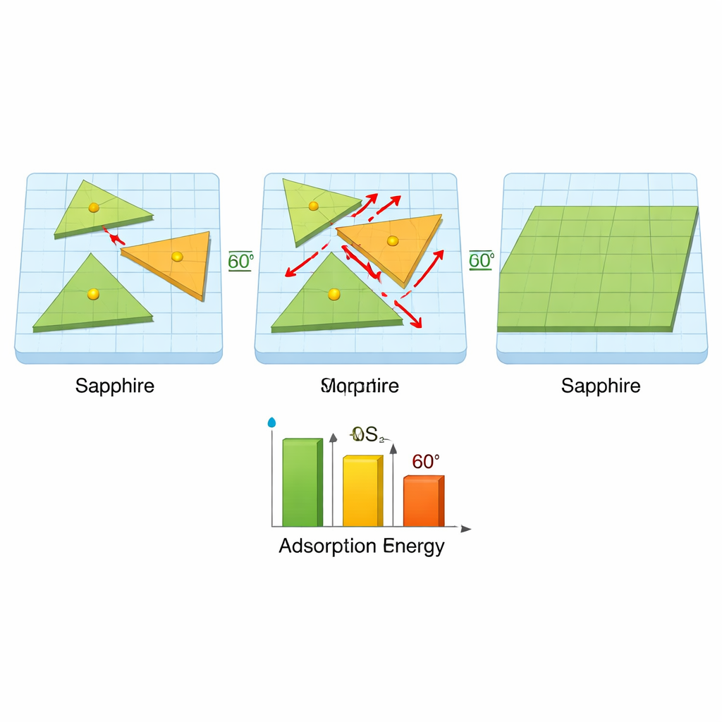
The authors introduce a different strategy using a common industrial tool called metal-organic chemical vapor deposition (MOCVD). They grow monolayer MoS₂ on commercially available sapphire wafers using a molybdenum oxychloride (MoO₂Cl₂) vapor and hydrogen sulfide gas. At first, many small triangular MoS₂ domains appear, including those rotated by 0°, 60°, and small “twist” angles in between. Careful X-ray and electron microscopy measurements reveal that these angles match a geometric pattern known as a coincidence site lattice, which describes how two different crystal grids can partially line up.
From Disordered Seeds to a Single Crystal Sheet
The surprising discovery is what happens as these islands grow and begin to touch. Instead of freezing in their original orientations, the misaligned and opposite domains gradually disappear. Grain boundaries—where two different orientations meet—move in such a way that material from the less favorable orientations is “eaten” and re-formed as the preferred 0° orientation. This process, called grain-boundary migration, is driven by tiny differences in how strongly each orientation sticks to the sapphire surface. Computer simulations show that the 0° alignment is slightly more stable in terms of energy, enough to bias the system so that, over time, almost the entire wafer becomes one continuous, unidirectional crystal.
Self-Limiting Growth: A Built-In Thickness Stopper
For electronics, having exactly one atomic layer is just as important as having a single crystal. Often, once the first layer is complete, extra material keeps piling up to form a second layer, ruining uniformity. Here, the chosen molybdenum source, MoO₂Cl₂, plays a crucial role: it does not readily stick to an existing MoS₂ surface, so once a complete monolayer forms, growth largely stops by itself over a wide range of times and conditions. Optical measurements, atomic force microscopy, and X-ray scans across 2-inch wafers all show that the film remains a single layer with highly uniform properties from edge to edge.
Proving Device Quality with Working Transistors
To show that this crystal quality matters in real circuits, the researchers transfer the monolayer MoS₂ from sapphire onto silicon wafers with oxide, then pattern many tiny transistors. These devices switch cleanly, with on/off current ratios of about ten million. More importantly, the speed at which electrons move through the material—its mobility—reaches about 66 cm²/Vs at room temperature and roughly 749 cm²/Vs at low temperature, figures that rival the best films grown by slower, less industrial methods. The way mobility changes with temperature also matches what is expected for clean, nearly grain-boundary-free crystals.
What This Means for Future Chips
In simple terms, the authors have shown how to grow a giant, seamless “sheet” of a promising 2D semiconductor on standard sapphire wafers, with a built-in mechanism that stops the film at exactly one atomic layer. Instead of having to perfectly control every seed crystal from the start, they let the system correct itself as it grows, guided by slight energy advantages. This self-aligned and self-limiting approach brings 2D materials a significant step closer to practical, wafer-scale integration in the next generations of low-power, ultra-small electronics.
Citation: Sakuma, Y., Atsumi, K., Hiroto, T. et al. Self-aligned and self-limiting van der Waals epitaxy of monolayer MoS2 for scalable 2D electronics. Nat Commun 17, 602 (2026). https://doi.org/10.1038/s41467-026-68320-8
Keywords: monolayer MoS2, 2D semiconductors, van der Waals epitaxy, wafer-scale growth, MOCVD