Clear Sky Science · en
Exciton-polariton photodiodes
Turning Light into Electrical Signals More Efficiently
Every time you take a photo, stream a movie over fiber optics, or use a remote control, you rely on photodiodes—tiny components that turn light into electrical signals. Today’s best photodiodes are made from classic semiconductors like silicon, but a new class of "excitonic" materials can absorb light far more strongly. The catch is that they usually move charges sluggishly, wasting much of that absorbed light. This article explores a new type of photodiode that borrows tricks from quantum optics to keep the strong absorption while dramatically improving how efficiently and how quickly light is converted to usable electrical current.
Why Regular Light Sensors Hit a Wall
In many modern solar cells and light sensors, incoming light first creates bound electron–hole pairs known as excitons. These excitons must travel to special interfaces inside the device before they can separate into free charges that contribute to current. Unfortunately, in most excitonic materials excitons can only diffuse short distances before they recombine and their energy is lost as heat or light. That short travel distance limits how thick the absorber layer can be, which in turn limits how much of the incoming light the device can realistically capture. Engineers are therefore stuck in a trade-off between absorbing more photons and actually collecting the resulting charges.
Blending Light and Matter into New Particles
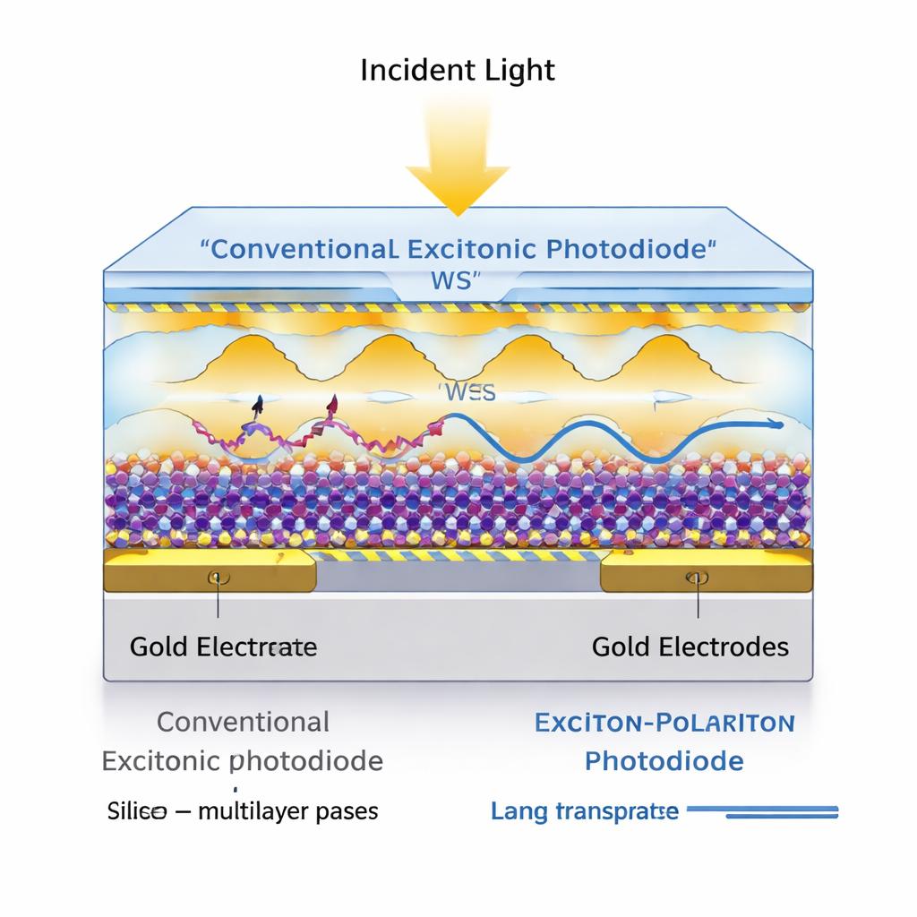
The researchers behind this work use a concept from quantum physics to escape that trade-off. When an excitonic material is placed inside an optical cavity—a structure where light bounces back and forth—it is possible for light and excitons to couple so strongly that they form new hybrid particles called exciton-polaritons. These hybrids behave partly like light, which is very light and can move quickly over long distances, and partly like matter, which can be turned into electrical current. In their devices, the team uses thin layers of the two-dimensional semiconductor WS2 sandwiched between metal contacts at the bottom and a transparent conducting film of tin-doped indium oxide (ITO) on top. The ITO not only collects charge but also acts as an anti-reflection coating, trapping light and naturally creating cavity modes inside the WS2 without any bulky mirrors.
Making Photons Work Harder Inside the Device
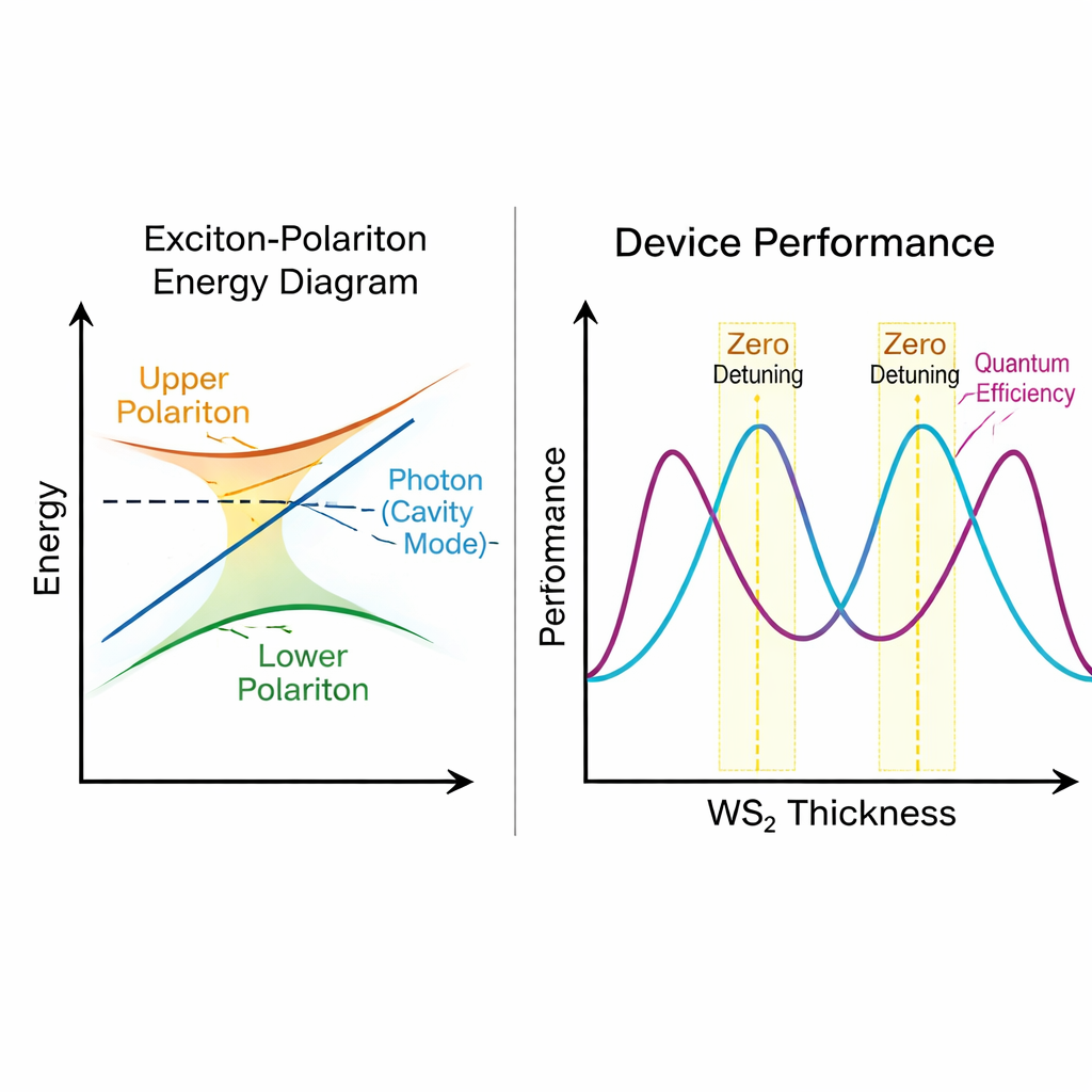
By carefully varying the thickness of the WS2 layer from a few nanometers to 200 nanometers, the researchers can tune the cavity’s internal light patterns so that they resonate with the natural exciton energy in WS2. At certain thicknesses, the resonance is just right—a situation called zero detuning—and strong light–matter coupling occurs. Experiments that measure how much light is reflected and how efficiently different colors generate current show clear signatures of polaritons: the optical spectrum splits into upper and lower branches, and the peaks in electrical response follow these branches as the thickness changes. Crucially for applications, the devices do not only respond at a single sharp color; thanks to the combination of the cavity and the large optical constants of WS2, they show strong, broadband absorption and can even harvest light just below the material’s usual band edge.
From Quantum Mixing to Real Performance Gains
To see whether these exotic hybrid states actually make better photodiodes, the team compares devices operating in a "weak" coupling regime with those showing strong polaritonic effects. As the WS2 thickness enters the strong-coupling range, both the external quantum efficiency (how many incident photons are turned into collected charges) and the internal quantum efficiency (how many absorbed photons in WS2 produce current) rise dramatically. Near the optimal thicknesses, the internal efficiency approaches unity—almost every absorbed photon contributes to current. At the same time, the devices maintain very low dark current, which keeps noise small, and reach responsivities comparable with or better than other exciton-based detectors. The polariton-assisted transport also speeds things up: response times drop into the few-hundred-nanosecond range, and the detectors can operate at megahertz-level modulation frequencies, suitable for high-speed optical communication.
What This Means for Future Light Detectors
For non-specialists, the key message is that the authors have shown a practical way to keep the strong light absorption of excitonic materials while overcoming their usual limitation of poor charge transport. By engineering devices in which light and excitons self-organize into fast-moving hybrid particles, they achieve photodiodes that are thin, broadband, efficient, and faster than most comparable technologies. The work suggests that future cameras, optical sensors, and even solar cells based on excitonic semiconductors might be designed not just by changing materials and layer thicknesses, but by deliberately shaping how light and matter are coupled at the quantum level inside the device.
Citation: Zhao, Q., Alfieri, A.D., Xia, M. et al. Exciton-polariton photodiodes. Nat Commun 17, 1607 (2026). https://doi.org/10.1038/s41467-026-68312-8
Keywords: exciton-polariton photodiode, strong light-matter coupling, transition metal dichalcogenide, quantum efficiency, ultrafast photodetector