Clear Sky Science · en
Laser-induced selective metallization of conductive patterns on silicone via copper carbonate hydroxide coating
Stretchy Wires for the Next Generation of Wearable Gadgets
From smartwatches to medical patches, many new gadgets need soft, skin-friendly wiring that can bend and stretch without breaking. But making metal circuits on squishy materials like silicone is surprisingly difficult: the metal usually doesn’t stick well, can crack when stretched, and often requires high heat or toxic chemicals to fabricate. This paper introduces a gentle, room‑temperature way to “draw” copper wiring directly onto a popular soft silicone rubber, opening the door to more reliable and comfortable wearable and implantable electronics.
Why Soft Electronics Are Hard to Build
Wearable devices and flexible sensors must hug the body, twist with joints, and survive thousands of stretches while still carrying clean electrical signals. Silicone rubbers such as Ecoflex are ideal for this job because they are extremely soft, stretchable, and biocompatible. However, their very low surface energy makes it hard for metal films or conductive inks to wet and stick to them. Existing approaches, like printing metal nanoparticle inks or embedding liquid metals, often require high‑temperature sintering, complicated surface treatments, or materials that can oxidize, detach, or irritate the skin. The field has lacked a simple, low‑toxicity method to pattern robust metal wiring onto pure silicone without turning it into a stiff, damaged composite.
A Laser “Drawing” Method on Soft Silicone
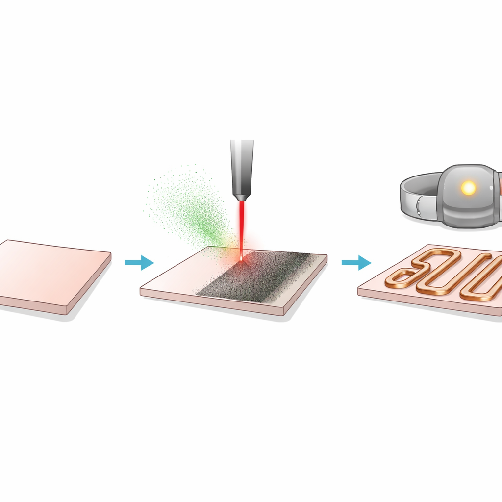
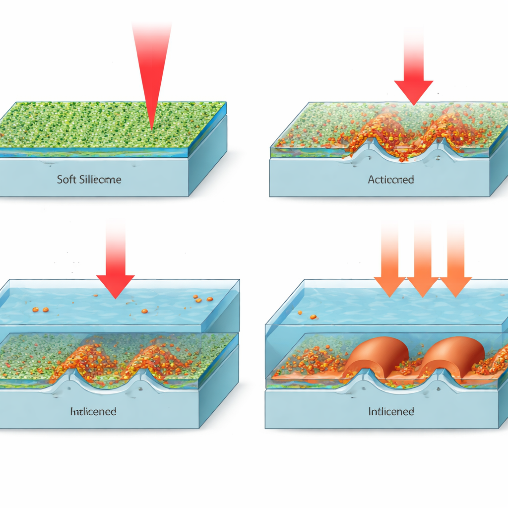
The researchers developed an updated process called laser‑induced selective metallization that works directly on cured Ecoflex silicone. First, they gently spray a thin layer of a green powder—copper carbonate hydroxide—onto the silicone surface. Then a near‑infrared laser scans only along the desired circuit routes. The laser energy locally heats the coating and the top of the silicone, roughening the surface, creating tiny carbon‑rich domains, and partly converting copper ions into metallic copper nanoparticles. These newly formed copper seeds lodge into the micro‑textured silicone, acting as anchors for the metal that will grow later. Unused powder can be washed off, collected, and reused, cutting waste and avoiding permanent loading of particles inside the silicone.
Growing Tough, Low‑Resistance Copper Paths
After laser treatment defines the “activated” paths, the sample is dipped into a chemical bath that deposits a thin copper layer only where seeds are present. This electroless plating step creates a continuous but relatively fragile metal film. To strengthen it, the team adds a low‑temperature electroplating step, which builds the copper up to about 30 micrometers thick. Microscopy and elemental analysis show how the initially smooth silicone becomes rough and then gradually covered with an increasingly dense copper layer. Mechanical tests reveal that the copper tracks are firmly locked into the silicone, with a peel strength far higher than many common flexible electrodes. By designing the copper in serpentine shapes, the researchers achieve stretchability up to about 125% strain while keeping electrical resistance changes very small over hundreds of stretch‑release cycles.
From Heart Signals to Flexible Antennas
To show that the process is practical, the team built several demonstration devices. They patterned copper traces on transparent Ecoflex to create a soft electrocardiogram (ECG) patch that adheres comfortably to the skin without extra adhesives. When worn by a volunteer, the patch captured clear heart signals for 30 minutes, both at rest and during gentle movement, with well‑defined waves needed for clinical interpretation. They also fabricated a stretchable circuit powering an array of blue LEDs that continued to shine while the silicone was bent and stretched, and a flexible wireless charging antenna that could wrap around a cylinder while still transmitting power. These examples suggest that the method can support real‑world use in wearable health monitors, soft lighting, and communication hardware.
What This Means for Everyday Technology
In simple terms, this work shows how to “print” tough copper wiring onto very soft silicone using only a recyclable powder, a scanning laser, and modest chemical baths—no masks, no high heat, and no expensive or highly toxic metals. The resulting circuits combine good electrical performance, strong attachment, and high stretchability, which are all essential for comfortable devices that live on or inside the body. With further improvements to protect copper from long‑term oxidation and to adapt the method to other plastics, this strategy could help make future wearables thinner, softer, and more reliable, bringing medical‑grade sensing and wireless functions closer to everyday clothing and skin‑like patches.
Citation: Wei, Y., Yang, X., Tian, H. et al. Laser-induced selective metallization of conductive patterns on silicone via copper carbonate hydroxide coating. Microsyst Nanoeng 12, 96 (2026). https://doi.org/10.1038/s41378-026-01207-2
Keywords: flexible electronics, stretchable electrodes, laser processing, copper plating, wearable sensors