Clear Sky Science · en
AI-driven feature recognition of SEM profiles in deep reactive ion etching based on physics-constrained variational autoencoder
Sharper Chips Through Smarter Imaging
Every smartphone, car airbag sensor, and medical microneedle depends on tiny three‑dimensional structures carved deep into silicon. Making these features clean, smooth, and repeatable is hard—and checking their quality under an electron microscope is even harder. This paper introduces a new artificial intelligence tool that can read these microscopic images automatically and far more accurately than humans, promising faster, cheaper, and more reliable production of advanced microdevices. 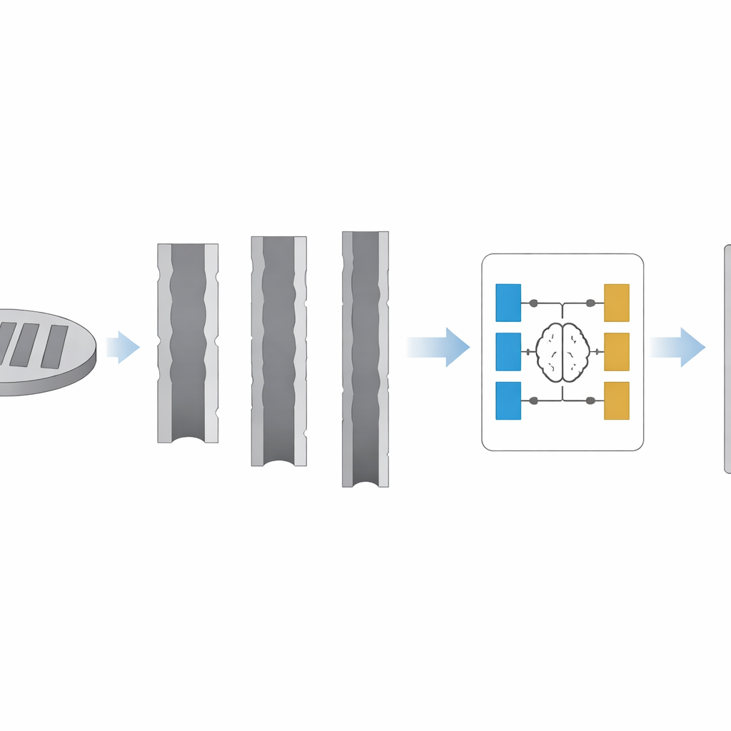
Why Etching Deep Tiny Grooves Is So Tricky
Modern microelectromechanical systems (MEMS) rely on deep, narrow trenches etched into silicon using a process called deep reactive ion etching. Engineers want walls that are almost perfectly vertical and smooth, but in practice the sidewalls develop ripples, bulges, and other distortions as the plasma alternates between carving and coating cycles. Small changes in timing, gas flow, temperature, or tool aging can turn a good recipe into a bad one, and these changes show up as subtle differences in the trench profile that are only visible in scanning electron microscope (SEM) cross‑sections.
The Bottleneck of Human Image Reading
Today, assessing these etched structures is mostly a manual craft. Engineers slice wafers, take hundreds of SEM images, and then painstakingly trace edges and measure depths and widths on a computer. Each image can take an hour or more to analyze, and different people often disagree by 15–20 percent on the same feature. Simple automatic methods and earlier machine‑learning tools like conventional neural networks can speed things up, but they struggle with the noisy, low‑contrast images typical of deep trenches and often miss how the structure changes with depth. As a result, image analysis has become a serious bottleneck for high‑throughput manufacturing and for using AI to optimize the etching process itself.
An AI That Respects the Physics
The authors propose a new approach called a physics‑constrained variational level set autoencoder, or VLSet‑AE. At its core, this AI system “compresses” a SEM image into a compact internal code and then “rebuilds” the shape of the trench from that code. Instead of treating the trench edge as just a set of bright pixels, it models the boundary as a moving interface that grows outward until it meets the real material, much like an expanding bubble that stops at the walls. The motion of this interface is guided by equations that describe how an etched surface should actually evolve in time, so the AI is steered not only by data but also by the known physics of the etching process. 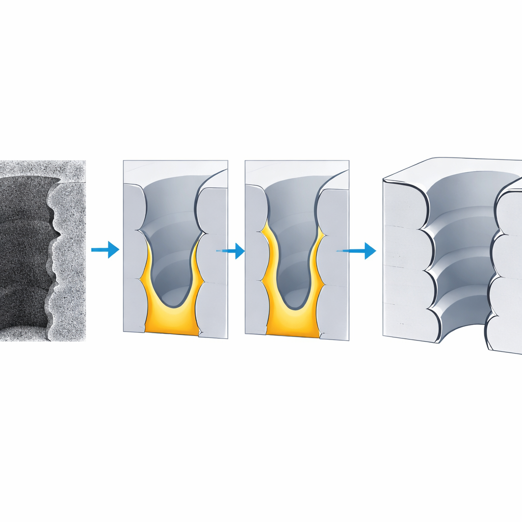
Seeing the Whole Trench in Space and Time
To train and test this system, the team designed a careful set of 16 etching recipes, varied the key cycle times that control how long the plasma carves and how long it protects, and collected 1,000 SEM cross‑section images. Each trench image was sliced into many thin layers along its depth, each representing one etch‑and‑coat cycle. VLSet‑AE tracks how the contour evolves layer by layer and then stitches these slices back together into a full three‑dimensional view. From this, it automatically calculates nine crucial measurements: the depth and width of the ripples on the wall, the local radius of curvature, how vertical the profile is, and the trench width at the top, middle, and bottom, along with the overall depth and bowing of the walls.
Faster, More Accurate, and Ready for the Factory
When compared with human measurements and seven other popular AI models, VLSet‑AE comes out on top. On average it disagrees with manual measurements by only about 3.7 percent—better than human‑to‑human variation—and reaches an overall recognition accuracy around 94–96 percent. It is also efficient: training on the full dataset takes on the order of tens of seconds, and analyzing a new image takes about a second. Even when tested with fewer training images, its accuracy degrades only slightly, showing that it can cope with limited data—a common situation in high‑end manufacturing.
What This Means for Everyday Technology
In simple terms, this work turns SEM inspection from an artisanal task into an industrial one. By automatically and reliably reading fine structural details from noisy microscope images, VLSet‑AE makes it practical to collect the huge volumes of data needed to let AI tune and monitor etching recipes in real time. That, in turn, can lead to smoother trenches, more precise sensors, and more consistent chips, all produced with less trial‑and‑error and lower cost. The method also offers a general blueprint for combining physics and machine learning to understand other complex manufacturing steps, pointing toward a future where micro‑ and nano‑devices are designed and perfected by tightly integrated, AI‑driven fabs.
Citation: Wang, F., Yu, H., Miao, Y. et al. AI-driven feature recognition of SEM profiles in deep reactive ion etching based on physics-constrained variational autoencoder. Microsyst Nanoeng 12, 82 (2026). https://doi.org/10.1038/s41378-025-01105-z
Keywords: deep reactive ion etching, scanning electron microscopy, physics-informed AI, variational autoencoder, microfabrication