Clear Sky Science · en
Generating polarized amplified spontaneous emission at high symmetry points of square lattices
Shaping Light on a Tiny Grid
Light is at the heart of everything from high‑speed internet to ultrasensitive sensors, but controlling it reliably on a scale smaller than the width of a human hair is still a major challenge. This study shows how carefully patterned metal films, drilled with orderly arrays of nanometer‑sized holes, can be used not only to guide and amplify light, but also to control its polarization—the direction in which its electric field wiggles. That level of control is crucial for future optical chips, secure communication, and compact sensing devices.
Metal Films as Nano Antennas
When light hits a metal surface that has been patterned with nanometer‑scale features, the electrons in the metal can slosh back and forth in unison, creating surface waves known as plasmons. In this work, the researchers use anodized aluminum oxide (AAO) membranes as very regular templates to make large, square lattices of nano‑holes in a metal film. By adjusting the processing steps, they turn each hole from a simple circle into a cross, and finally into a combined circle‑plus‑cross shape. Even though these changes are tiny—only a few hundred nanometers across—they strongly affect how surface waves move across the film and how they turn back into light.
Dialing Down Symmetry to Tune Polarization
The key idea is that the simpler, more symmetric a repeating pattern is, the more restricted its optical behavior becomes. The team deliberately reduces the symmetry of each unit in the square lattice: first a perfectly round hole, then a cross‑shaped hole, then a more lopsided circle‑plus‑cross pair. They study special points in the lattice’s momentum diagram—called high‑symmetry points—where light waves interact most strongly with the patterned metal. Using a custom imaging setup that maps angles of light into a camera image, they measure how the polarization direction of the emitted light changes at these points as the hole shape becomes less symmetric. One central point shows a 45‑degree rotation of polarization, while four others show a full 90‑degree flip as symmetry is lowered.
Finding the Sweet Spot for Polarized Emission
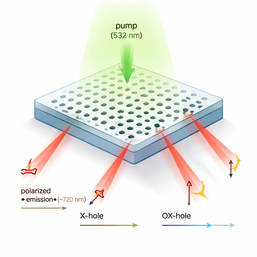
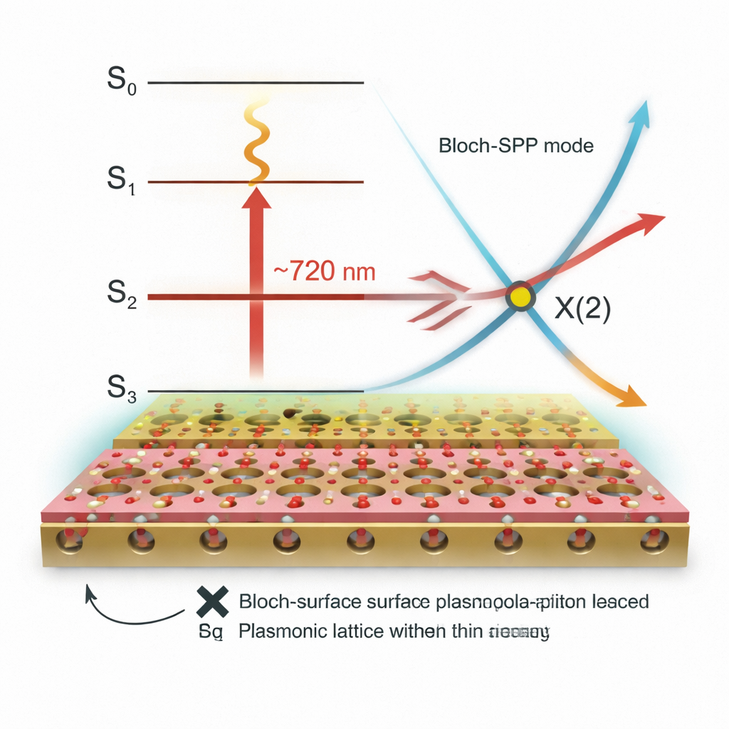
Among all the lattice designs, the circle‑plus‑cross (called the OX‑hole) stands out. At a particular high‑symmetry point labeled X(2), the lattice supports a surface wave whose energy lines up with red light around 720 nanometers. At this point, the degree of polarization—a measure of how strongly the light favors one direction over others—reaches 0.59, meaning the emission is highly polarized rather than random. Because the AAO templates can cover centimeter‑scale areas with nearly perfect ordering, these effects are not confined to tiny lab samples; they can, in principle, extend across practical device sizes without being washed out by defects.
Turning Dye Molecules into Directional Nano Light Sources
To turn this structured metal film into an active light source, the researchers coat it with a thin layer of a fluorescent dye called Nile Red, which naturally emits over a broad red band. They then shine green laser light at 532 nanometers onto the structure. When the dye’s emission around 720 nanometers overlaps with the lattice’s surface wave at the X(2) point, the surface wave feeds energy back into the dye layer, amplifying certain photons more than others. The result is amplified spontaneous emission: a bright, narrowed, partially laser‑like output. On the OX‑hole lattice, the emission becomes about four times stronger than on plain glass, its spectral width shrinks, and its polarization becomes strongly directional and elliptically shaped, all once the pump power crosses a clear threshold.
Why This Matters for Future Photonic Devices
In everyday terms, this work shows how “carving” metal films with carefully arranged nano‑holes can turn a simple glowing dye into a compact, bright, and highly polarized light source with built‑in directionality. By linking hole shape, lattice symmetry, and specific points in the momentum diagram, the authors provide a design playbook for tuning polarization and amplification without changing the dye or the pump laser. Such tunable, polarized nano‑emitters could form the building blocks of future optical sensors, on‑chip light sources, and communication components that are faster, smaller, and more efficient than today’s electronics‑based technologies.
Citation: Wang, T., Wang, Y., Wu, Y. et al. Generating polarized amplified spontaneous emission at high symmetry points of square lattices. Microsyst Nanoeng 12, 73 (2026). https://doi.org/10.1038/s41378-025-01023-0
Keywords: plasmonic lattices, polarized emission, nanohole arrays, amplified spontaneous emission, nanophotonics