Clear Sky Science · en
Single-pulse lithography of amorphous photonic architectures inside all-inorganic dielectric crystals
Writing Light Paths Inside Crystal
Imagine being able to “draw” tiny circuits for light directly inside a clear crystal, the way a laser printer writes ink on paper—only in three dimensions, and in a single shot. This research shows how to do just that: using one ultra-short laser pulse to sculpt invisible, glassy sheets inside solid crystals that can reshape light with record-breaking efficiency. The work points toward far smaller, tougher optical components for communications, sensing, and quantum technologies, all hidden safely inside transparent materials.
Why Bother Sculpting Inside Crystals?
Modern information systems increasingly rely on light rather than electrons, because light can carry more data faster and with less heat. The catch is that most photonic devices today are built on flat surfaces: patterns etched on chips, thin films, or waveguides. That is like trying to design a skyscraper using only one floor. Crystals such as lithium niobate and quartz have exceptional optical properties and are already used in telecom and laser systems, but their strong atomic bonds make them very hard to pattern internally with standard lithography. The authors tackle this roadblock by turning small regions of these crystals into an amorphous, glass-like phase whose optical behavior is very different from the surrounding crystal, enabling strong control over how light moves and changes color inside the bulk material.
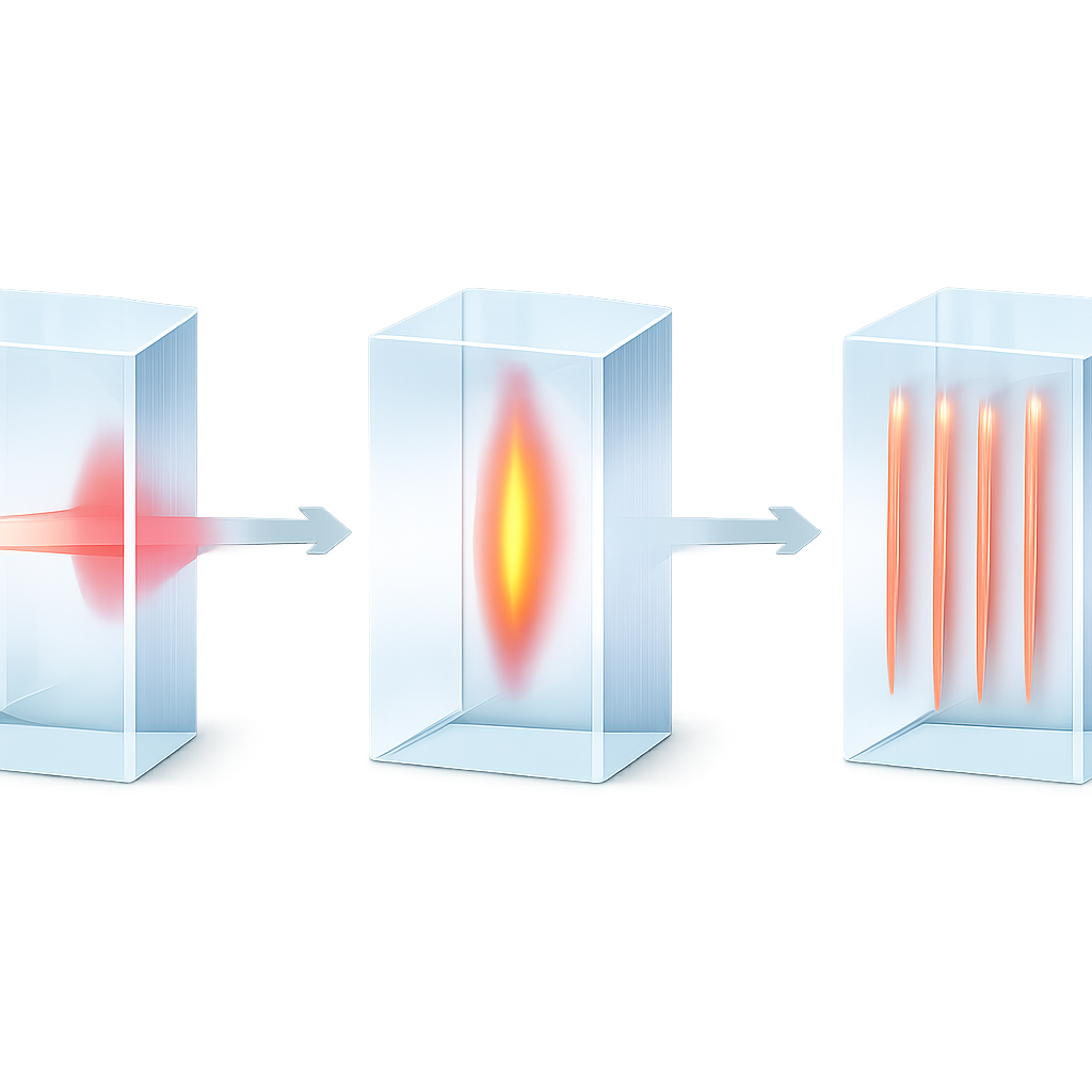
One Laser Shot, Big Structural Change
The core innovation is a process the authors call single-pulse anisotropic amorphization lithography. A single, tightly focused ultrafast laser pulse is aimed into the crystal. Although the crystal barely absorbs ordinary light, the extreme intensity at the focus generates a dense cloud of free electrons, driving the material in that tiny volume into a transient, metal-like state. These electrons carry heat much more effectively in one direction than in others, so the deposited energy spreads unevenly, elongating along a chosen axis. As the hot region cools in millionths of a second, that narrow zone solidifies into an amorphous sheet embedded in the still-crystalline surroundings. By shaping the laser beam or the crystal orientation, the team can steer the direction, length, and aspect ratio of these sheets, reaching structures as thin as 200 nanometers yet tens of micrometers long.
Tuning Shape, Direction, and Materials
Because the effect is driven by a single pulse, it avoids many of the defects and irregularities that plague multi-pulse laser writing, such as unwanted cracks or fine interference patterns. The authors show they can rotate the amorphous sheets to arbitrary angles, stretch them using slit-shaped beams, and achieve aspect ratios up to about 190 to 1—like inscribing a razor-thin ribbon inside the crystal. Microscopy and electron imaging confirm a clean boundary between the amorphous and crystalline regions, with high structural uniformity. Importantly, the same strategy works not just in lithium niobate but also in quartz, lithium tantalate, yttrium orthovanadate, and other dielectric crystals, indicating a broadly applicable platform rather than a one-material trick.
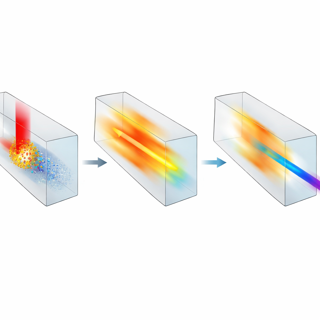
Turning Hidden Structures into Light Converters
These buried glassy sheets act as powerful, precisely arranged regions where the crystal’s nonlinear response is switched off. By carefully choosing their spacing and thickness, the researchers engineer conditions under which different colors of light reinforce each other as they propagate—a strategy known as quasi-phase matching. In lithium niobate, they build compact three-dimensional gratings that convert an incoming infrared beam into green light carrying twisted, vortex-like wavefronts. The conversion efficiencies reach around 1.7% overall for second-harmonic light, far surpassing previous internal beam-shaping schemes in similar materials. In quartz, which is normally a weak nonlinear performer, they stack fork-shaped patterns to generate both second and third harmonics simultaneously, achieving about 3% and 0.1% efficiency, respectively—the highest nonlinear beam shaping performance reported in a single quartz crystal.
Robust, Compact, and Ready for 3D Photonics
Because the patterned regions are fully enclosed by hard, inorganic crystals, the devices are mechanically durable and thermally stable, surviving heating to 1000 °C with only modest performance loss. The structures occupy areas as small as tens of micrometers, making them promising building blocks for dense three-dimensional photonic circuits that can sit alongside existing optical components. In essence, the authors demonstrate a new way to write clean, high-contrast optical functions directly into the interior of common crystals, using just one carefully tuned laser pulse per feature. For non-specialists, the takeaway is that we are moving from flat, surface-bound optics to truly volumetric, sculpted light paths inside solid materials—an advance that may underpin the next generation of compact, energy-efficient optical technologies.
Citation: Wang, Z., Ma, R., Lin, H. et al. Single-pulse lithography of amorphous photonic architectures inside all-inorganic dielectric crystals. Light Sci Appl 15, 177 (2026). https://doi.org/10.1038/s41377-026-02253-1
Keywords: ultrafast laser lithography, amorphous photonic structures, nonlinear frequency conversion, 3D integrated photonics, lithium niobate and quartz crystals