Clear Sky Science · en
Over 1.65 GW cm−2 sr−1 brightness 590 nm yellow second-harmonic generation in MOCVD-grown high-strain InGaAs/GaAs quantum well VECSEL
Why bright yellow light matters
Yellow lasers may sound like a niche technology, but they are quietly enabling some of today’s most advanced science and medicine. Yellow light is ideal for cooling atoms close to absolute zero, guiding giant telescopes as they peer deep into the universe, probing the human eye, and even treating certain skin and vascular diseases. Yet building compact, reliable yellow lasers that are both powerful and sharply focused has remained surprisingly difficult. This paper reports a major step toward mass‑produced yellow lasers that are bright, efficient, and practical outside specialized laboratories.
From infrared chips to yellow beams
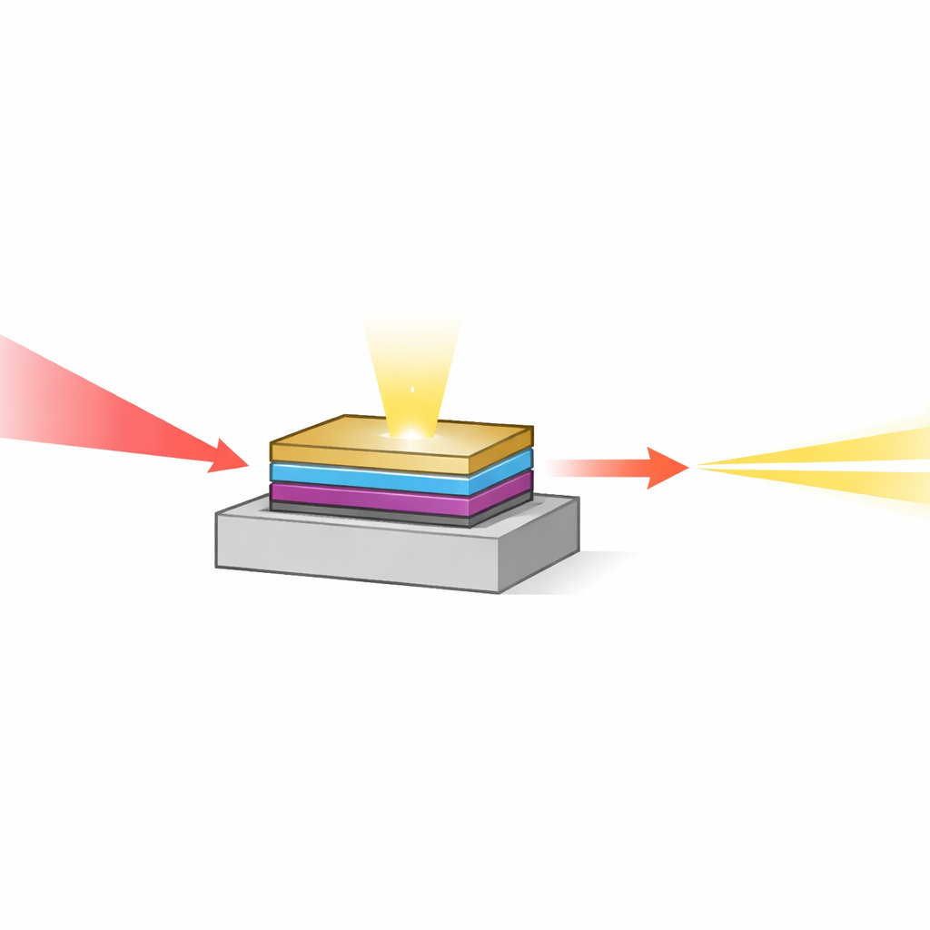
Instead of trying to build a yellow laser directly, the researchers start with a semiconductor device that emits invisible infrared light at around 1.2 micrometers in wavelength. This device is a vertical external‑cavity surface‑emitting laser, or VECSEL: a thin, mirror‑backed chip that is pumped by another laser and sits inside an open optical cavity. Inside the cavity, a nonlinear crystal converts the infrared light to its second harmonic—roughly half the original wavelength—which lands in the yellow at about 590 nanometers. By combining a powerful infrared source with efficient frequency doubling, the team aims to create a compact system that rivals or beats bulkier solid‑state and fiber‑based yellow lasers.
Engineering the tiny light factories
At the heart of the chip are ultra‑thin layers called quantum wells, made of indium gallium arsenide (InGaAs) sandwiched between gallium arsenide (GaAs). These wells are where light is actually generated. To reach the desired infrared color, the wells must contain a high fraction of indium, which stretches the crystal and builds up mechanical strain. If that strain is not carefully managed, the crystal relaxes by forming defects that scatter light and sap efficiency. The authors use a “flip‑chip” design with eight quantum wells and a stack of mirror layers beneath them, carefully positioning the wells where the internal light field is strongest so that each well contributes effectively to the gain.
Taming strain and wandering atoms
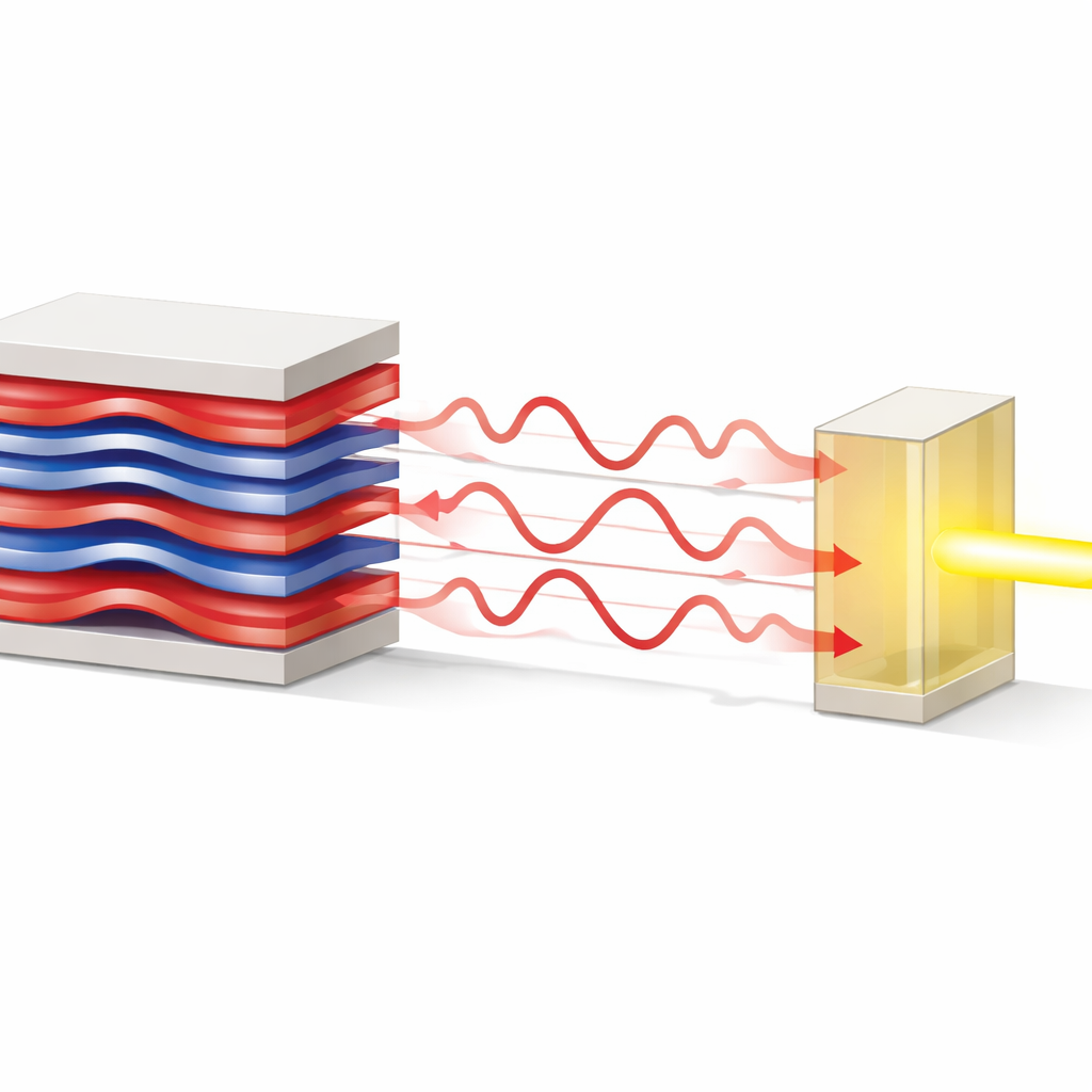
A central challenge is that indium atoms tend to drift during growth and heating, leading to uneven composition—an effect called segregation. The team tackles this by adding a compensating layer of gallium arsenide phosphide (GaAsP), which is under opposite strain, and by inserting a thin GaAs layer between InGaAs and GaAsP to reduce unwanted mixing. Crucially, they compare two growth strategies in a metal‑organic chemical vapor deposition (MOCVD) reactor, a method well‑suited to high‑volume manufacturing. In the first approach, all active layers are grown at a relatively low temperature to hold indium in place. This suppresses defects initially, but the structure degrades when later heated, losing indium and optical quality.
A smarter temperature recipe
In the improved strategy, the indium‑rich wells are still grown at low temperature, but the GaAsP layers are grown at higher temperature, with a GaAs spacer layer used during the temperature ramps. This “variable‑temperature” recipe lets phosphorus incorporate more effectively, giving stronger strain compensation and smoother interfaces. High‑resolution microscopy and X‑ray measurements show that indium is now evenly distributed across the wells, surfaces are flatter, and internal layer boundaries are sharper. After annealing, the emission color shifts only slightly and remains narrow, indicating good thermal stability—crucial for a laser that must endure strong pumping and long‑term operation.
From lab‑grade chip to bright yellow source
With the optimized structure, the packaged VECSEL chip produces more than 45 watts of continuous infrared power at low coolant temperatures, with over 50% slope efficiency—exceptionally strong performance for an MOCVD‑grown device in this wavelength range. When placed in a carefully designed V‑shaped cavity containing a nonlinear crystal, the infrared light is converted into continuous yellow output exceeding 6.2 watts. The beam is almost perfectly diffraction‑limited, meaning it can be tightly focused, and the resulting brightness reaches about 1.65 gigawatts per square centimeter per steradian—a figure on par with or better than many bulkier solid‑state and fiber lasers. The yellow output also shows promising stability over time.
What this means going forward
To a non‑specialist, the key message is that the authors have shown how to grow and process complex semiconductor laser chips, using industry‑friendly methods, to produce remarkably bright and clean yellow beams. By fine‑tuning how layers are stacked, strained, and heated during growth, they suppress defects that previously limited performance. Although molecular beam epitaxy, a slower and more expensive technique, still holds some performance records, this work narrows the gap while offering a clear path to mass production. In practical terms, it brings compact, efficient yellow lasers much closer to widespread use in astronomy, precision measurements, imaging, and medical therapy.
Citation: Zhang, Z., Zhan, W., Xiao, Y. et al. Over 1.65 GW cm−2 sr−1 brightness 590 nm yellow second-harmonic generation in MOCVD-grown high-strain InGaAs/GaAs quantum well VECSEL. Light Sci Appl 15, 161 (2026). https://doi.org/10.1038/s41377-026-02230-8
Keywords: yellow lasers, VECSEL, second-harmonic generation, semiconductor epitaxy, adaptive optics