Clear Sky Science · en
Harnessing diverse hybrid integration for bridging trans-scale multi-dimensional fiber-chip data transmission and processing
Why Future Internet Pipes Need a New Kind of Bridge
Every video call, cloud backup, and AI training run depends on light zipping through hair-thin glass fibers and tiny on-chip circuits. But today there is a hidden bottleneck: data races quickly along long-distance optical fibers, only to hit slower, power-hungry electronics when it reaches processing hardware in data centers and network nodes. This paper shows a new way to directly connect high-capacity optical fibers to advanced photonic chips, shrinking that bottleneck and pointing toward much faster, more efficient communication networks.
From Long-Haul Cables to Tiny Chips
Modern networks increasingly rely on "multi-lane" light, where information is packed into many dimensions at once: different colors (wavelengths), polarizations, and spatial patterns (modes) of light. Few-mode fibers can carry several such spatial modes, dramatically boosting capacity over long distances. On the other end, silicon photonic chips can route, filter, and process light on scales of millimeters using dense on-chip waveguides. But these two worlds do not naturally match: the light patterns inside fiber cores look very different from the modes in nanometer-scale chip waveguides. Today’s solutions often require multiple intermediate conversions, racks of equipment, and repeated optical–electrical–optical steps that burn energy and add delay.
Building a Bridge Across Scales
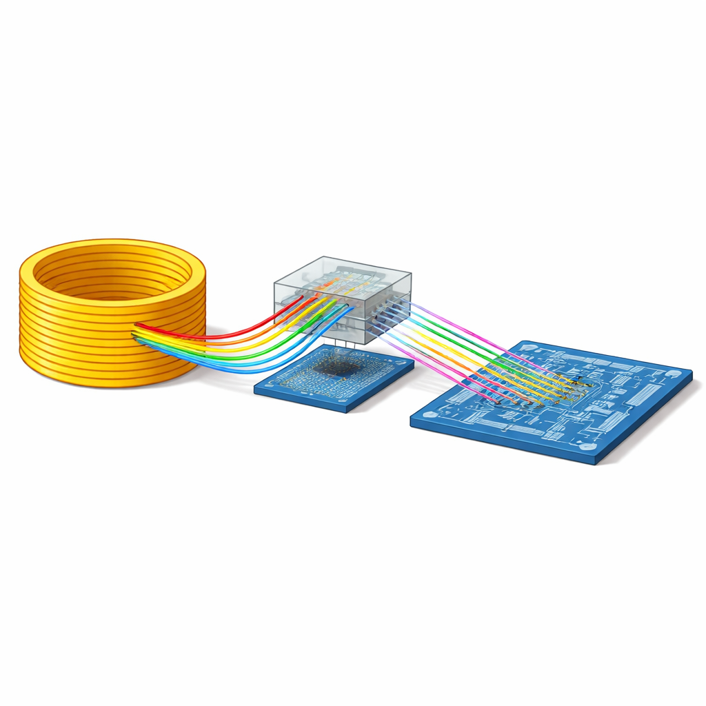
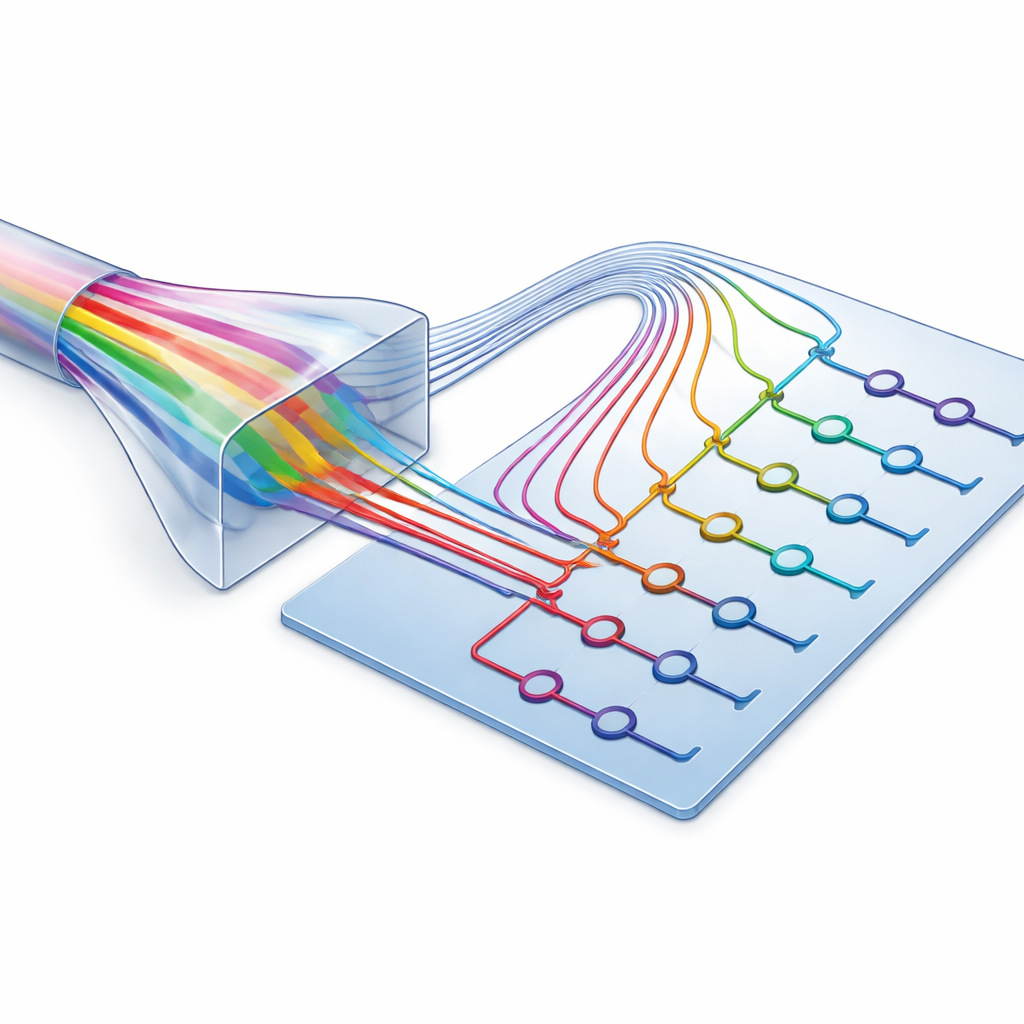
The authors propose a hybrid "bridge" that combines a three-dimensional glass chip with a two-dimensional silicon photonic circuit. Instead of trying to directly match complex multi-mode patterns between the fiber and the chip, the bridge first transforms the light into a tidy array of simple single-mode channels. In the glass section, different spatial patterns (modes) from the few-mode fiber are carefully separated using a specially shaped coupler and routed into distinct single-mode waveguides, all written in 3D using femtosecond laser pulses. These single-mode paths then hand off the light to the silicon chip through tapered connections designed for low loss and good tolerance to fabrication variations.
Turning Optical Highways into Reconfigurable Grids
Once on the silicon chip, the separated channels are reshaped into the modes that the on-chip multimode waveguides use. Additional structures on the chip split and rotate polarizations so that everything can be processed using a common, well-controlled fundamental mode. The heart of the processing engine is a large reconfigurable optical add–drop multiplexer (ROADM) built from arrays of tiny ring-shaped resonators. By slightly heating these rings, the team can shift which colors of light they interact with, allowing specific wavelength channels to be added to or removed from the data stream on demand. More than 2,000 individual components—crossings, couplers, heaters, and contact pads—are integrated on a single silicon die to realize 192 distinct channels spanning three spatial modes, two polarizations, and 32 wavelengths.
Putting the System to a Realistic Test
To show that this is more than a lab curiosity, the researchers built a full transmission experiment. They generated 32 wavelength channels, each carrying a high-speed data signal using a common advanced modulation format. These signals were divided among six spatial and polarization combinations, launched into a few-mode fiber, passed through the hybrid 3D/2D coupler, and routed by the on-chip ROADM. At the output, a coherent receiver and digital processing recovered the data. Across all 192 channels, the measured error rates stayed below standard forward-error-correction thresholds at practical optical signal-to-noise levels, corresponding to an overall throughput of about 20 terabits per second. Tests with longer fiber lengths showed only modest performance penalties, and the wide tuning range of the resonators allowed channels to be reassigned if any port failed, improving robustness.
What This Means for the Next Internet
In essence, this work closes two gaps at once: the physical size gap between thick long-haul fibers and tiny on-chip waveguides, and the performance gap between ultra-fast optical transmission and slower electronic processing. By combining 3D glass waveguides, 2D silicon photonics, and a highly reconfigurable on-chip switching fabric, the authors demonstrate a scalable architecture that can move and manipulate huge volumes of data without constantly reverting to electronics. While further improvements in loss, scaling, and functionality are possible, this 192-channel, 20-terabit-per-second fiber-chip system is a strong step toward future communication networks where light stays in the optical domain from the backbone cable all the way into the processing chip.
Citation: Li, K., Yan, G., Wang, K. et al. Harnessing diverse hybrid integration for bridging trans-scale multi-dimensional fiber-chip data transmission and processing. Light Sci Appl 15, 167 (2026). https://doi.org/10.1038/s41377-026-02194-9
Keywords: silicon photonics, optical fiber networks, mode-division multiplexing, reconfigurable optical add-drop multiplexer, terabit data transmission