Clear Sky Science · en
Fourier ptychographic coherence scanning interferometry for 3D morphology of high aspect ratio and composite micro-trenches
Peering into Tiny Deep Trenches
Modern microchips and sensors are filled with ultra-narrow, ultra-deep grooves—microscopic trenches that can be 300 micrometers deep yet only about 10 micrometers wide. Their exact three-dimensional shape strongly affects how devices like pressure sensors, advanced LEDs, and meta-optics perform. Until now, seeing these hidden shapes clearly has meant either damaging the sample or accepting blurry, incomplete measurements. This paper introduces a new optical method that looks through the material instead of bouncing light off it, revealing crisp 3D maps of these deep features without cutting anything open.
Why Deep Grooves Matter
These high-aspect-ratio trenches—very deep compared with their width—are workhorses of miniaturized technology. In tiny machines called MEMS, they create flexible springs and comb-like structures for measuring pressure or motion. In advanced LEDs and optical components, they guide light and increase efficiency. However, their performance depends sensitively on details such as how smooth the bottom is, how straight the sidewalls are, and whether the depth and width match the design within a fraction of a micrometer. Industry often relies on electron microscopes for such checks, but those require slicing or otherwise damaging the sample, which is impractical for routine, in-line inspection.
Limits of Today’s Optical Tools
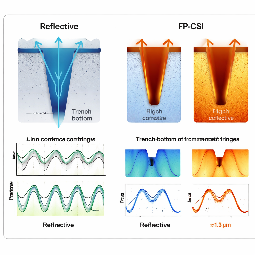
Non-destructive optical methods try to solve this by using light instead of cutting, but they have struggled with these extreme geometries. A leading technique, coherence scanning interferometry, shines broadband light onto a surface and analyzes interference fringes to build a height map. For shallow, open structures this works well. But in deep and narrow trenches, light reflects and scatters multiple times between steep walls. The result is washed-out fringes and noisy signals, especially at the trench bottom, precisely where engineers need reliable measurements. Using weaker, low-angle illumination can improve signal clarity but at the cost of blurring fine details, forcing a trade-off between resolution and reliability.
Looking Through Instead of Just At
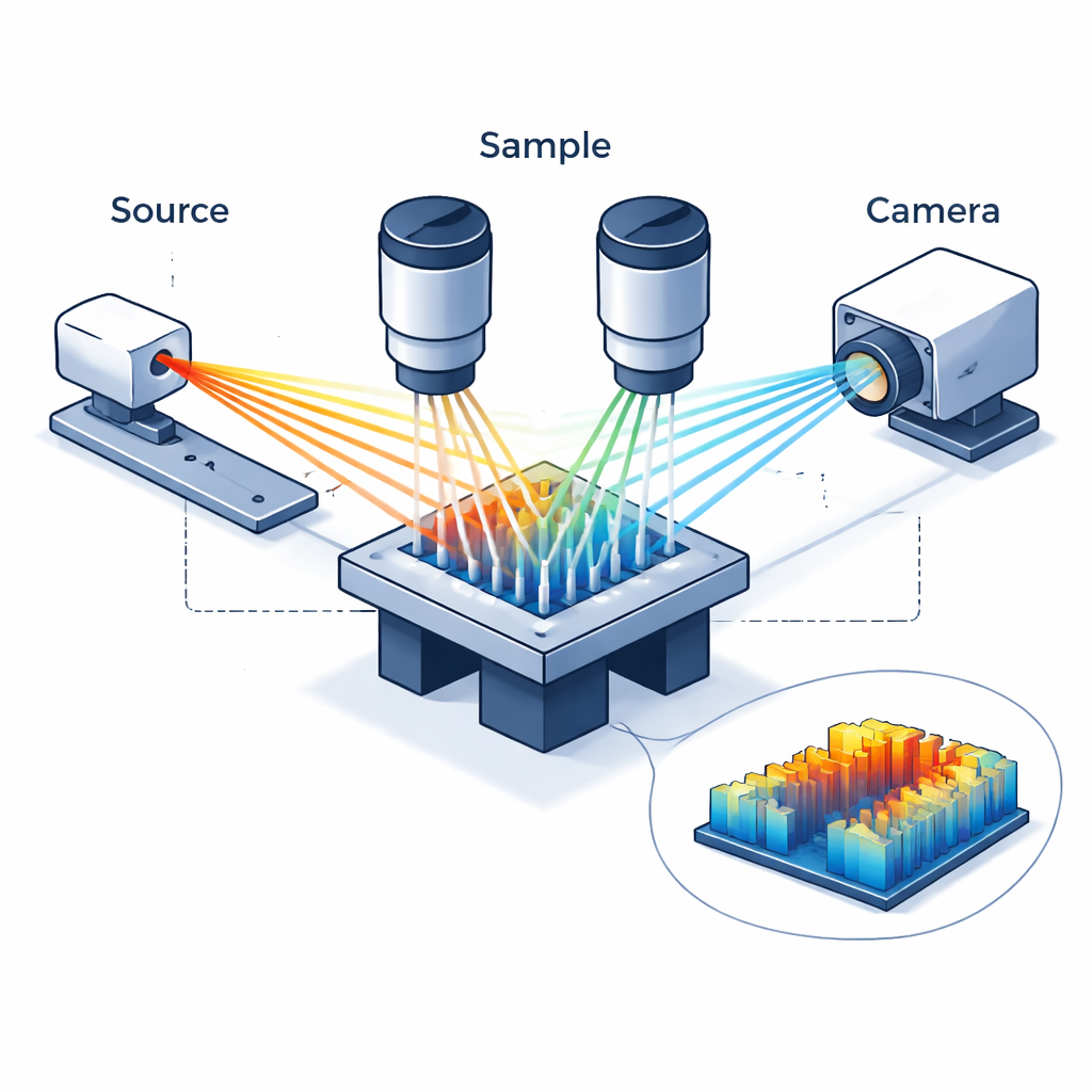
The authors’ approach, called Fourier ptychographic coherence scanning interferometry (FP-CSI), changes the geometry of the measurement. Instead of reflecting light off the sample, the system sends near-infrared light through a transparent silicon wafer in a carefully balanced interferometer. A tiny illumination spot is shifted sideways so that the sample is probed by many slightly different angles of almost parallel light. Because the light passes through the structure only once and at small divergence, the signal is far less distorted, and the interference fringes stay strong even at the bottom of very deep trenches. The method then corrects subtle distortions in the recorded signals and combines the many angled views in the frequency domain, effectively stitching together a larger optical aperture and recovering fine details without heavy, iterative computations.
Sharp 3D Maps of Real Devices
Using FP-CSI, the team measured single silicon trenches 300 micrometers deep with widths as small as 10 micrometers, as well as complex multilayer MEMS pressure sensors containing multiple trench levels. In all cases, the method produced detailed three-dimensional maps that closely matched cross-check measurements from electron microscopy, but without any sample damage. Width and depth errors were around one percent or less over repeated trials. The system could resolve line features only 1.3 micrometers apart—essentially at the fundamental resolution limit set by the optics—and, crucially, maintained nearly this level of sharpness at the bottom of model trenches with aspect ratios greater than 10:1, where standard reflective interferometers largely failed.
What This Means for Future Manufacturing
For non-specialists, the key message is that FP-CSI offers a way to “see” the exact 3D shape of extremely deep and narrow grooves inside transparent microdevices quickly and without cutting them open. By combining the strengths of two previously separate imaging ideas—interference-based height measurement and multi-angle synthetic imaging—the technique overcomes a long-standing compromise between clarity and reliability. This makes it a promising tool for next-generation semiconductor fabrication, MEMS manufacturing, and other micro-optoelectronic systems where invisible tiny shapes determine whether a device passes or fails.
Citation: Li, Y., Yuan, Q., Huo, X. et al. Fourier ptychographic coherence scanning interferometry for 3D morphology of high aspect ratio and composite micro-trenches. Light Sci Appl 15, 93 (2026). https://doi.org/10.1038/s41377-026-02189-6
Keywords: 3D optical metrology, micro-trenches, MEMS inspection, interferometry, semiconductor manufacturing