Clear Sky Science · en
In-situ formation of oriented perovskite nanosheets with tailored optical dipoles enabling >30% EQE in pure-red LEDs
Brighter Red Screens for Everyday Devices
From smartphones to virtual-reality headsets, our lives are filled with tiny lights that create vivid images. The quest is to make these lights—especially pure, deep reds—brighter, more energy-efficient, and longer-lasting. This paper shows how carefully arranging the tiny crystal layers inside a new class of materials called perovskites can dramatically boost the performance of red light-emitting diodes (LEDs), pushing them close to the practical limits of efficiency for next-generation displays.
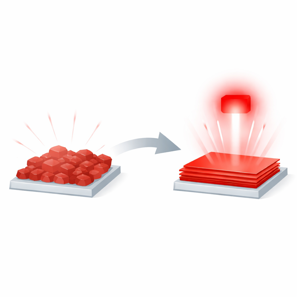
From Messy Crystal Grains to Tidy Layers
Perovskite semiconductors have quickly become star materials for LEDs because they can be made from solution, like inks, yet still shine with very pure colors. However, when these materials are coated as thin films, their light-producing units—known as optical dipoles—tend to point in random directions. In flat, planar devices, this disorder means much of the light gets trapped instead of escaping outward. As a result, even though red perovskite LEDs have recently reached external quantum efficiencies (EQEs) above 25%, they still lag behind top organic LEDs and are theoretically capped near 30% efficiency if nothing is done about this disorder.
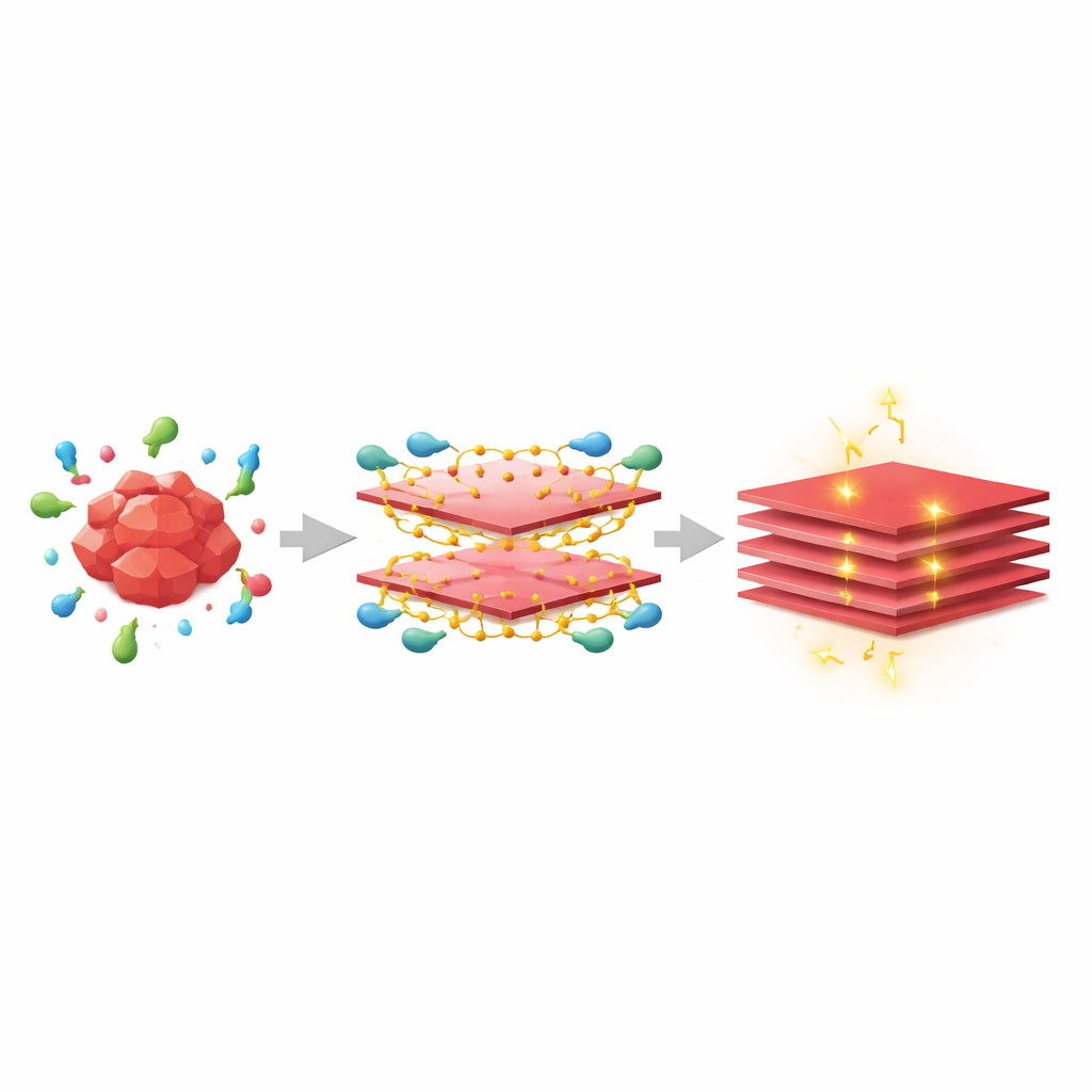
Guiding Crystal Growth with Smart Molecules
The authors tackle this problem by redesigning how the perovskite crystals grow inside the film. They focus on “quasi-two-dimensional” perovskites that naturally form layered structures, like stacks of nanosheets. The trick is to use special organic molecules, called ligands, that sit between the inorganic layers and steer the way the crystals assemble. By swapping a widely used naphthalene-based ligand (1-NMA) for a closely related cousin (2-NMA), they exploit subtle differences in molecular shape and how these molecules stack together. Computer calculations show that 2-NMA lowers the energy barrier for forming flat nanosheets, while experiments confirm that it binds more strongly and more neatly to the perovskite framework, encouraging ordered layer-by-layer growth directly in the film.
Building Perfect Nanosheets Inside the Film
Using 2-NMA, the team observes a clear transformation. Instead of irregular, grainy crystals with leftover lead iodide, the perovskite film now contains clean, face-on nanosheets stacked in an orderly fashion. Advanced imaging methods reveal uniform crystal spacing and strong in-plane orientation, while X-ray scattering patterns change from smeared rings (signaling random structures) to sharp spots (indicating well-aligned layers). This architecture does more than just look tidy: it reorients the light-emitting dipoles so that 86% lie horizontally—much higher than the 68% in conventional films. That orientation alone is predicted to boost how much light escapes from a planar device by roughly 20%.
More Light, Fewer Losses, Faster Charges
The nanosheet design also cleans up the electronic landscape of the film. Measurements show that the density of defects—tiny imperfections that swallow light and electrical charges—drops by more than a factor of two compared with conventional films. The photoluminescence quantum yield, a measure of how many absorbed photons are re-emitted as light, climbs above 90%, and the average light-emission lifetime grows longer, consistent with fewer nonradiative losses. At the same time, despite the presence of organic layers, the films maintain charge-carrier mobility comparable to that of fully three-dimensional perovskites, meaning charges can still move swiftly through the material. Together, these factors create a film that both transports charges efficiently and turns them into light with very little waste.
Record-Setting Red LEDs and What Comes Next
When built into devices, these oriented nanosheet films deliver pure-red LEDs at 635 nm with a record EQE of 31.2%, matching detailed optical simulations that factor in both orientation and material brightness. The devices also shine more brightly—reaching over 13,000 candelas per square meter—switch on at lower voltage, and last far longer than their conventional counterparts, with operational lifetimes extended by more than tenfold. By showing that careful molecular design can sculpt crystal orientation and dipole alignment directly during film formation, this work offers a broadly applicable blueprint for high-efficiency, solution-processed light sources, lasers, and integrated photonic components—not just better red pixels, but a new way to engineer light from the bottom up.
Citation: Liu, S., Zhang, D., Wang, L. et al. In-situ formation of oriented perovskite nanosheets with tailored optical dipoles enabling >30% EQE in pure-red LEDs. Light Sci Appl 15, 163 (2026). https://doi.org/10.1038/s41377-026-02184-x
Keywords: perovskite LEDs, red light emission, nanosheet crystals, ligand engineering, display technology