Clear Sky Science · en
Femto-joule threshold reconfigurable all-optical nonlinear activators for picosecond pulsed optical neural networks
Why Tiny Bursts of Light Could Power Future AI
Today’s artificial intelligence runs on vast farms of power-hungry electronic chips. As we demand smarter phones, cars, and data centers, electricity use and heat are becoming major roadblocks. This paper reports a way to do some of that heavy lifting with light instead of electrons, using tiny optical devices that act like the “activation” switches in a neural network. These switches work with incredibly small light energies and at blistering speeds, offering a glimpse of ultrafast, energy‑efficient AI hardware.
From Slow, Hot Electronics to Fast, Cool Photonics
Conventional computer chips move electrical charges through metal wires and transistors. That approach has served us well, but it is reaching limits in both speed and energy efficiency. Optical neural networks replace moving charges with photons traveling in waveguides—essentially tiny on‑chip light paths. Light can carry information rapidly, in many colors at once, and with little heating. However, building a practical all‑optical neural network requires a key ingredient: a compact device that takes in a light signal and outputs a transformed version of it in a nonlinear way, just as a neuron in the brain fires only when the input passes a threshold. Until now, such all‑optical “activation” elements have tended to be too large, too slow, or too power‑hungry.
A Microscopic Light Trap That Learns to Bend Signals
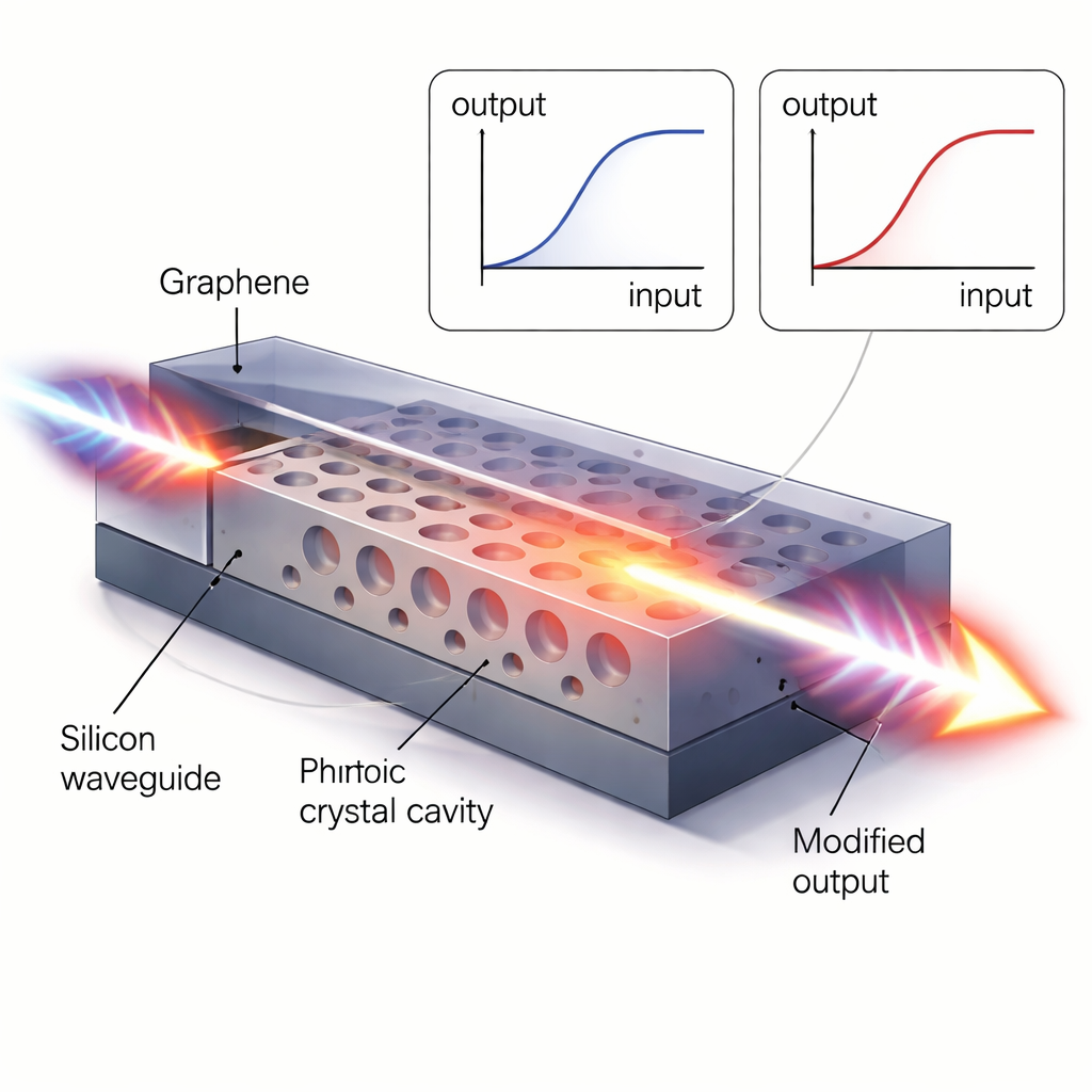
The authors first engineer a silicon photonic crystal cavity—a perforated slab of silicon that traps and slows down light at specific colors. By carefully arranging a row of holes, they create a tiny region where a short light pulse can resonate, building up its intensity. This boosts a subtle property of silicon called the Kerr effect, where the material’s refractive index changes slightly when the light inside becomes intense. That small change nudges the cavity’s preferred color and, as a result, alters how much of a passing light pulse gets through. By choosing the input wavelength relative to the cavity’s resonance peak, the researchers can make the device behave like several different activation curves used in machine learning, including linear, ReLU‑like (rectified linear), and sigmoid‑like responses. Even in this purely silicon version, the activator is only about 15 micrometers by 10 micrometers—smaller than a grain of dust—and responds in under 2 trillionths of a second.
Adding Graphene for Ultra‑Low Energy Switching
To drive the activation threshold even lower, the team integrates a single‑atom‑thick layer of graphene on top of the silicon cavity. Graphene naturally absorbs light, but at high intensities its absorption saturates: once many electrons are excited, additional photons can pass more easily. By combining this “saturable absorption” with the cavity’s slow‑light enhancement, the device reaches a saturation energy of only 4 femtojoules—roughly the energy carried by a few tens of thousands of telecom photons—and a response time of about 1 picosecond. At nearby wavelengths, the same structure can still exploit silicon’s Kerr effect to reshape its activation curve on demand, switching between sigmoid‑like, ReLU‑like, and nearly linear behaviors with thresholds as low as 30 femtojoules. In terms of speed and required energy, this figure of merit beats previous on‑chip optical activators by several orders of magnitude.
Building a Pulsed Optical Brain on a Chip
Using these activators as building blocks, the authors outline a full optical neural network architecture driven by ultrafast light pulses rather than continuous beams. A high‑repetition‑rate pulsed laser generates a train of picosecond spikes, which are encoded with data by high‑speed modulators and then split across many wavelengths. On chip, specialized wavelength‑division components route and weight these colors using nonvolatile phase‑change materials that remember their settings without consuming power. After linear weighting, the signals pass through the graphene‑silicon activators, which imprint the desired nonlinear response before the light is routed to the next layer. Simulations show that, with activation energies below about 30 femtojoules, such a system could reach computational densities around 10³ trillion operations per second per square millimeter and energy efficiencies near 10⁶ trillion operations per watt per square millimeter—far beyond typical electronic accelerators.
What This Means for Everyday AI
To test whether these exotic optical activations behave like their electronic counterparts, the team feeds their measured activation curves into software models and trains them on standard classification tasks, from simple two‑dimensional patterns to handwritten digits (MNIST) and complex color images (CIFAR‑10). The graphene‑silicon activations match or outperform simple linear responses, particularly on the harder image tasks, where ReLU‑like behavior proves especially powerful. In plain terms, this work shows that a thumbnail‑sized chip of carefully structured silicon and graphene could one day handle key steps in AI calculations using tiny bursts of light instead of electricity. If scaled and integrated with mature photonic technologies, such all‑optical nonlinear activators could help deliver faster, cooler, and more efficient hardware for the next generations of artificial intelligence.
Citation: Liu, R., Wang, Z., Zhong, C. et al. Femto-joule threshold reconfigurable all-optical nonlinear activators for picosecond pulsed optical neural networks. Light Sci Appl 15, 128 (2026). https://doi.org/10.1038/s41377-025-02175-4
Keywords: optical neural networks, graphene photonics, photonic crystal cavities, nonlinear activation, energy-efficient AI hardware