Clear Sky Science · en
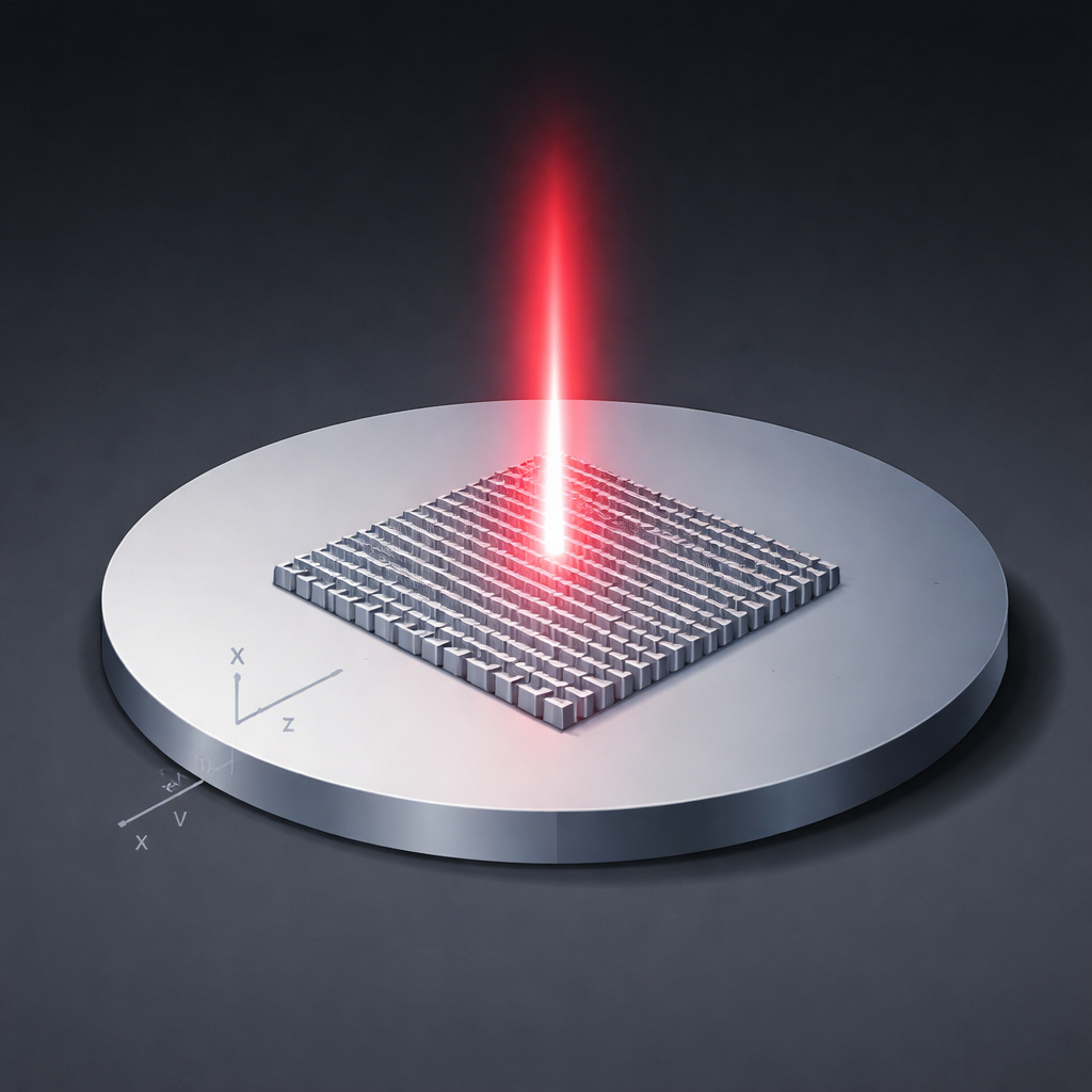
One-dimensional photonic crystal nano-ridge surface emitting lasers epitaxially grown on a standard 300 mm silicon wafer
New Tiny Lasers for Silicon Chips
Lasers are the unseen workhorses inside data centers, smartphones, and sensors. Yet today’s most common tiny lasers, called VCSELs, are difficult to make in many colors and do not integrate easily with the silicon chips that run our electronics. This research demonstrates a new kind of microscopic laser, grown directly on a standard 300 mm silicon wafer, that could make on-chip light sources cheaper, more versatile, and easier to scale.
Why Current Chip Lasers Fall Short
Vertical-cavity surface-emitting lasers (VCSELs) are popular because they are compact and can be tested directly on the wafer. However, they rely on thick stacks of precisely grown mirror layers and work best only at a few standard wavelengths, such as 850 and 980 nanometers. Shifting them to the longer wavelengths needed for telecommunications or sensing is difficult and costly. Making many different wavelengths on the same wafer is even harder, and directly combining VCSELs with conventional silicon-based electronics is rarely done. These limitations motivate the search for laser designs that are simpler to grow, easier to tune, and naturally compatible with silicon manufacturing.
Building Lasers from Nano-Ridges
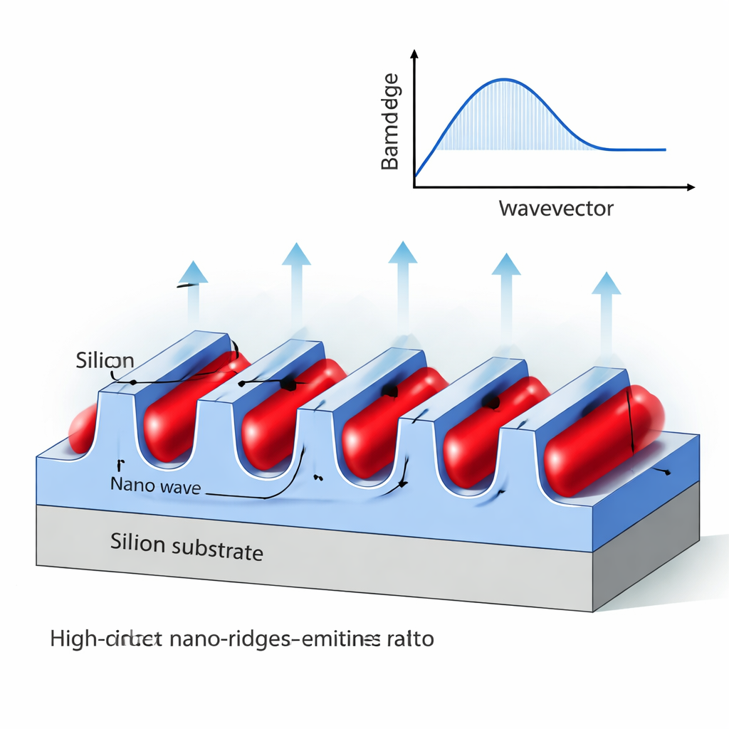
The authors use a technique called aspect ratio trapping and nano-ridge engineering to grow high-quality light-emitting material directly on patterned silicon. Instead of forming a continuous layer, the active material forms a regular array of extremely narrow, tall strips known as nano-ridges. This built-in pattern behaves like a one-dimensional photonic crystal: the repeating sequence of high-index ridges and air gaps strongly shapes how light can travel. By carefully choosing the ridge height, width, and spacing, the team designs a “slow-light” mode at the edge of the photonic band—the point where light effectively crawls along the structure. This slow, standing wave provides strong optical feedback, allowing the array itself to act as the laser cavity while sending light straight up from the chip surface.
Trapping Light for Efficient Operation
The key physical trick is to exploit so‑called bound states in the continuum, special optical modes that sit in a frequency range where radiation is allowed but remain trapped because of symmetry. In an ideal infinite array, some of these modes would never leak out. In a real, finite device, slight imperfections and finite size break the symmetry just enough to allow controlled vertical emission while keeping the optical losses low. Simulations show which modes couple best to the nano-ridge quantum wells and how their color shifts when the ridge width, period, or height is changed. The most important parameters turn out to be the ridge width and spacing, which can tune the emission across the gain band of the material, roughly from 980 to 1060 nanometers, without changing the underlying semiconductor recipe.
From Design to Working Devices
To turn the infinite-array concept into compact pixels, the team defines finite sections of nano-ridge arrays and surrounds them laterally with “mirror” regions. Instead of changing the period, they slightly modify the refractive index by filling nearby gaps with a transparent material, which shifts the local photonic band and reflects light back into the central cavity. Experiments on many devices with different cavity sizes reveal how the laser threshold depends on width: wider cavities generally have lower thresholds because they confine light better, but past about 35 micrometers the benefit saturates and disorder starts to matter. The best devices show room‑temperature lasing with thresholds as low as 5–10 kilowatts per square centimeter, narrow spectral lines, strong polarization along the ridges, and clean, narrow beams with angular spreads under about 10 degrees.
What This Could Mean for Future Technologies
In simple terms, the authors have shown that rows of tiny semiconductor ridges, grown directly on a standard silicon wafer, can act as efficient surface‑emitting lasers whose color is set mainly by geometry. Because the approach reuses mainstream silicon processing, it is well suited to large‑scale manufacturing and to co‑integration with photonic and electronic circuits. By adjusting material composition, the same platform could be extended from near‑infrared data‑com links to longer wavelengths used in LIDAR, environmental sensing, and spectroscopy. With future work on electrical injection and electrode design, these nano‑ridge surface‑emitting lasers could become practical on‑chip light sources across a wide range of applications.
Citation: Fahmy, E.M.B., Ouyang, Z., Colucci, D. et al. One-dimensional photonic crystal nano-ridge surface emitting lasers epitaxially grown on a standard 300 mm silicon wafer. Light Sci Appl 15, 120 (2026). https://doi.org/10.1038/s41377-025-02061-z
Keywords: silicon photonics, surface emitting lasers, photonic crystals, nano-ridge lasers, integrated optoelectronics